Contactless IC card adhered with layers for showing holographic and laser images

a technology of laser images and contactless ic cards, which is applied in the field of contactless ic cards adhered with layers for showing laser images, can solve the problems of increasing the general production cost, weak emission frequency, increasing material and labor costs, etc., and achieves the effect of strengthening the surface effect of printed images, less frequency loss, and good surface

Inactive Publication Date: 2019-02-07
HONG BAOLI
View PDF0 Cites 0 Cited by
  • Summary
  • Abstract
  • Description
  • Claims
  • Application Information

AI Technical Summary

Benefits of technology

[0008]A thickness of the metal-plated layer will affect light penetration, light reflection and electrical conductivity. The thicker the metal-plated layer is, the lesser the light can penetrate and the better the light reflection and electrical conductivity will be. On the contrary, the thinner the metal plated layer is, the more the light can penetrate and the light reflection and electrical conductivity will get worse. As compared to 380 ű50 Å being a thickness of a corresponding layer according to the existing holographic imaging technique, the metal-plated / nano material layer advantageously has a thickness of 150±50 Å, thereby maintaining the same holographic and laser effect and at the same time reducing frequency loss such that the IC card can be readable within a longer distance. A (Angstrom) is a unit measuring a thickness of an aluminum plated layer. 1 Å=10−10 m=0.1 nm.
[0009]Preferably, the holographic PET / PVC laser plastic layer also comprises a laser coating layer, positioned between the metal-plated / nano material layer and the PET / PVC base film layer; the laser coating layer is an image layer that reflects specific variable images at any selected portion of the card depending on viewing angle and lighting; the metal-plated / nano material layer is a coating layer of electrochemical aluminum, and is printed with images by laser; images printed on a laser PVC material show a glittering effect when viewed in different angles; changeable images and different colors are observed, and specific variable images can be seen at any selected portion of the card. Thus, the visual effect is good, and the anti-forgery and anti-scanning and replication ability of a transaction card can be enhanced, thereby being safer to use.
[0010]Preferably, the lower card structure also comprises the same holographic polyester (PET) / polyvinyl chloride (PVC) laser plastic layer, the same printing layer and the same PET / PVC film layer sequentially arranged on the IC chip, with the holographic PET / PVC laser plastic layer being the nearest to the IC chip and the PET / PVC film layer being farthest away from the IC chip. Therefore, both sides of the IC card have holographic and laser effect.
[0012]Preferably, the metal-plated / nano material layer is made with laser mold pressing rainbow holographic images and texts by utilizing laser color hologram plate making technique and mold pressing replication technique. Visible or invisible images, texts or messages are made on the IC card. Since color patches in a hologram are randomly combined, it is difficult to create two identical templates even using the same equipment. Therefore, a rainbow hologram can be used as an anti-forgery label. A laser mold pressing holographic anti-forgery label has four kinds of coloring, namely a single rainbow color, multiple rainbow colors, true color and black and white (achromatic color); the laser mold pressing holographic anti-forgery label can have a 2D image, a 3D image, multiple layers of images or be made with dynamic imaging. There is a type of gilded hologram and also a see-through type hologram, the latter one allows images and texts covered by the hologram to be readable when they are observed through the hologram; therefore, this type of see-through hologram is also called transparent hologram. Another type of see-through hologram is provided with multiple layers of transparent medium plated on the patterns of the hologram, so that the hologram is only visible under a specific viewing angle; when the viewing angle changes, an almost transparent film is visible that reveals the images and texts originally covered by the hologram. This another type of see-through hologram is even more advantageous than the first described see-through hologram.
[0014]The present invention has the following beneficial effects compared with prior art: A contactless integrated circuit (IC) card adhered with layers for showing holographic and laser images, taken into account the relationship between readable distance, reading success rate and surface effect, solving the problem of weak emission frequency of the chip after a holographic laser film and a PVC card are adhered together, and strengthening surface effect of printed images in card making industry. The IC card of the present invention is readable within a long distance, has lesser frequency loss, can be manufactured by mass production, has a good surface effect, has a long service life and possesses good anti-forging ability. The IC card of the present invention has a wide range of applicability in different fields that may use IC card.

Problems solved by technology

However, this method will result in exceptionally weak emission frequency.
Therefore, there is an increase in material and labor costs for production, thereby increasing the general production cost, lowering the production efficiency and increasing defective product rate.

Method used


Image

  • Contactless IC card adhered with layers for showing holographic and laser images
  • Contactless IC card adhered with layers for showing holographic and laser images
  • Contactless IC card adhered with layers for showing holographic and laser images

Examples


embodiment 1

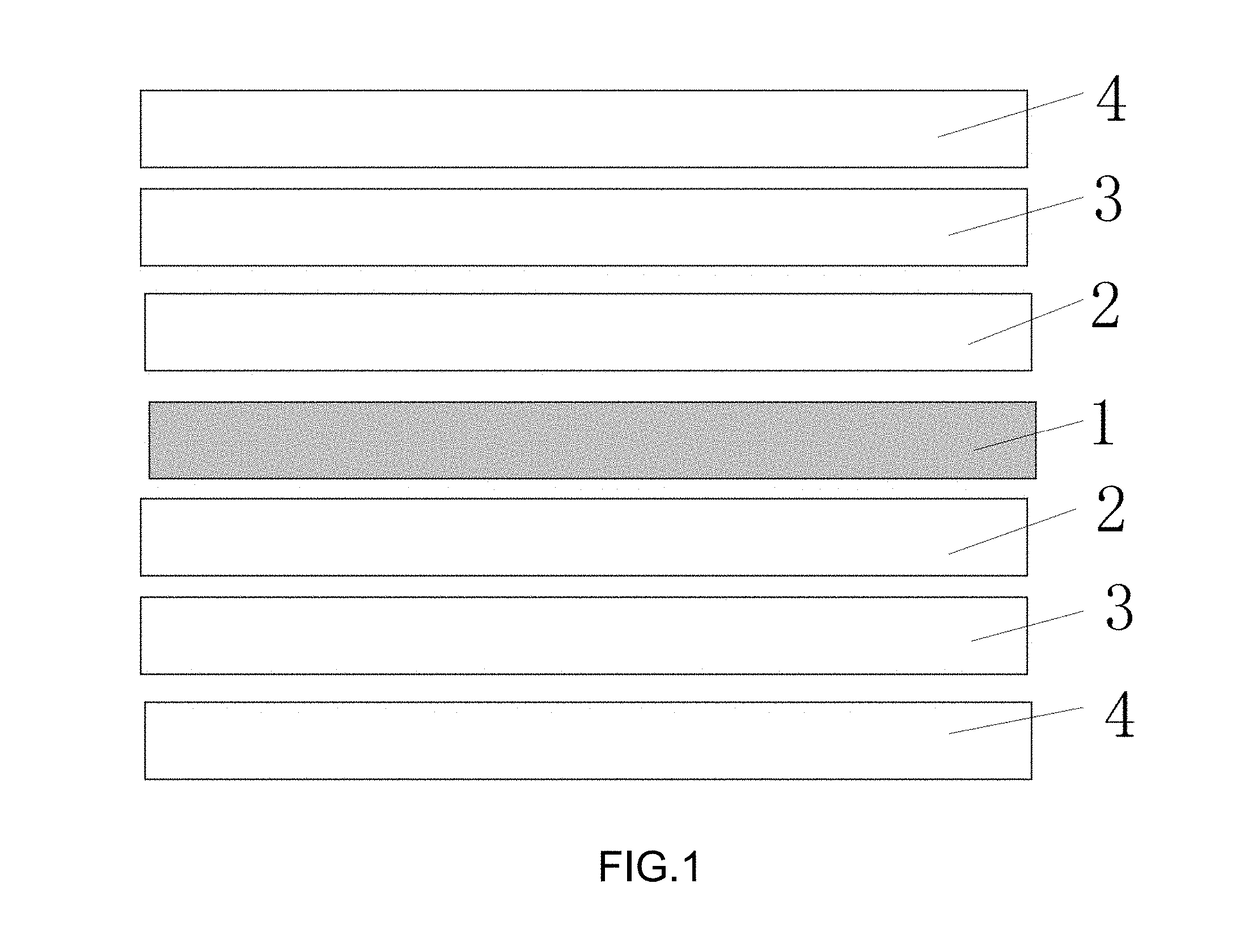
[0021]As shown in FIGS. 1-2, a contactless IC card adhered with layers for showing holographic and laser images comprises an integrated circuit (IC) chip 1 and a card structure; the IC chip 1 is disposed inside the card structure; the card structure comprises an upper card structure and a lower card structure; the upper card structure comprises a holographic polyester (PET) / polyvinyl chloride (PVC) laser plastic layer 2, a printing layer 3 and a PET / PVC film layer 4 sequentially arranged on the IC chip 1, with the holographic PET / PVC laser plastic layer 2 being the nearest to the IC chip 1 and the PET / PVC film layer 4 farthest away from the IC chip 1; the holographic PET / PVC laser plastic layer 2 is responsible for showing holographic and laser images; the printing layer 3 has images printed thereon, and the PET / PVC film layer 4 protects the holographic PET / PVC laser plastic layer 2 and the printing layer 3.

[0022]The holographic PET / PVC laser plastic layer 2 comprises a PET / PVC plas...

embodiment 2

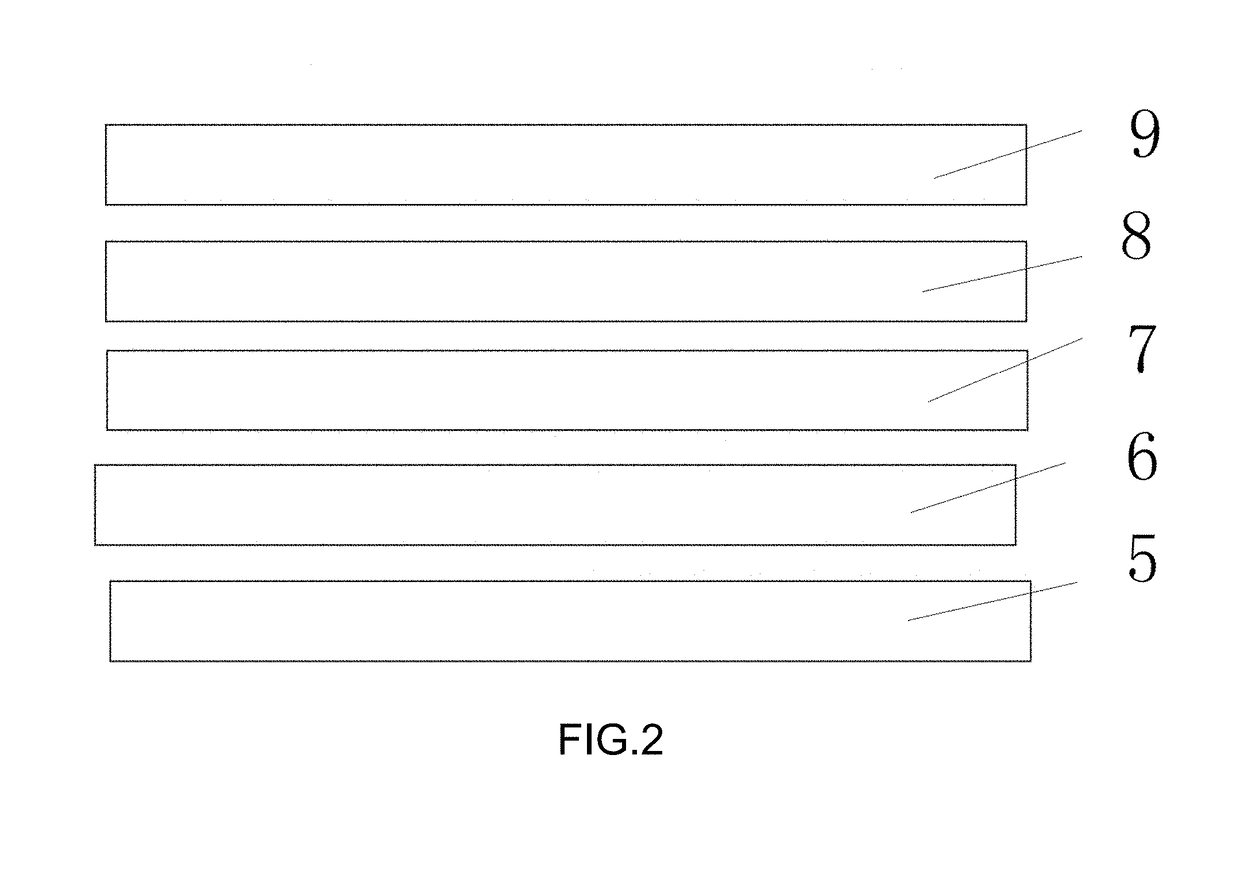
[0027]With reference to FIG. 4, embodiment 2 is different from embodiment 1 in that, the lower card structure comprises a PET / PVC plastic layer 5, a printing layer 3 and a PET / PVC film layer 4 sequentially arranged on the IC chip 1, with the PET / PVC plastic layer being nearest to the IC chip 1 and the PET / PVC film layer being farther away from the IC chip 1. In other words, the lower side of the IC card does not have any holographic or laser effect.

[0028]In a testing under the same testing conditions, and given that the metal-plated / nano material layer is an aluminum plated layer, an IC card applying the holographic technique of the prior art having a thickness of a corresponding layer being 380 ű50 Å has a maximum readable distance of 35-40 mm when only a single side of the card is used, and a maximum readable distance of 25-30 mm when both sides of the card are used. The IC card according to the present invention has a maximum readable distance of 40-45 mm which is 5±2 mm more th...


PUM

PropertyMeasurementUnit
distanceaaaaaaaaaa
emission frequencyaaaaaaaaaa
readable distanceaaaaaaaaaa

Abstract

A contactless integrated circuit (IC) card adhered with layers for showing holographic and laser images, having an IC chip and a card structure; the IC chip is disposed inside the card structure; the card structure has an upper card structure and a lower card structure; the upper card structure has a holographic polyester (PET) / polyvinyl chloride (PVC) laser plastic layer, a printing layer and a PET / PVC film layer sequentially arranged on the IC chip, with the holographic PET / PVC laser plastic layer being the nearest to the IC chip and the PET / PVC film layer farthest away from the IC chip; the holographic PET / PVC laser plastic layer is responsible for showing holographic and laser images; the printing layer has images printed thereon, and the PET / PVC film layer protects the holographic PET / PVC laser plastic layer and the printing layer.

Description

BACKGROUND OF THE INVENTION[0001]The present invention relates to the making of integrated circuit cards, and more specifically relates to a contactless IC card adhered with layers for showing holographic and laser images.[0002]An integrated circuit (IC) card has a card shape by inserting a microelectronic chip into a card base according to ISO 7816. An IC card can have a contact interface, a contactless interface or a contact and contactless dual interfaces, classified according to the type of communication interface the IC card uses. A contactless IC card is also called a RFID card, which comprises an IC chip and a sensor antenna, and is encapsulated within a standard PVC card; the IC chip and the antenna are not exposed to the external environment. Therefore, contactless IC card is a ground breaking product in the field of electronic components in being passive (no power source in the card) and contactless. A contactless IC card is highly reliable, easy to use, anti-collision (th...

Claims


Application Information

Patent Timeline
Patent Type & Authority Applications(United States)
IPC IPC(8): G06K19/077B32B7/12B32B27/36B32B27/30
CPCG06K19/07722B32B7/12B32B27/36B32B27/304G06K19/07749B32B2457/00B32B2425/00G06K19/06065G06K19/0723B32B27/06B32B2307/75B32B2307/402B32B2255/205B32B2250/05B32B2307/416B32B2307/202B32B2307/412
Inventor HONG, BAOLI
Owner HONG BAOLI
Why Eureka
Try Eureka