Methods for forming a semiconductor structure and related semiconductor structures

a semiconductor structure and semiconductor technology, applied in the direction of semiconductor devices, basic electric elements, electrical appliances, etc., can solve the problems of difficult to obtain advantageous ultra-shallow junctions, large integration and device design challenges, and use of bulk materials other than silicon

Active Publication Date: 2019-05-02
ASM IP HLDG BV
View PDF22 Cites 243 Cited by
  • Summary
  • Abstract
  • Description
  • Claims
  • Application Information

AI Technical Summary

Problems solved by technology

As semiconductor devices continue to decrease in size in advanced technology nodes, a number of challenges arise in developing higher performance devices.
However, using a bulk material other than silicon presents a huge integration and device design challenge.
For example, diffusion enhancement of n-type dopants in germanium (Ge) makes it very challenging to obtain advantageous ultra-shallow junctions.
Moreover, the major

Method used


Image

  • Methods for forming a semiconductor structure and related semiconductor structures
  • Methods for forming a semiconductor structure and related semiconductor structures
  • Methods for forming a semiconductor structure and related semiconductor structures

Examples


Embodiment Construction

[0014]Although certain embodiments and examples are disclosed below, it will be understood by those in the art that the invention extends beyond the specifically disclosed embodiments and / or uses of the invention and obvious modifications and equivalents thereof. Thus, it is intended that the scope of the invention disclosed should not be limited by the particular disclosed embodiments described below.

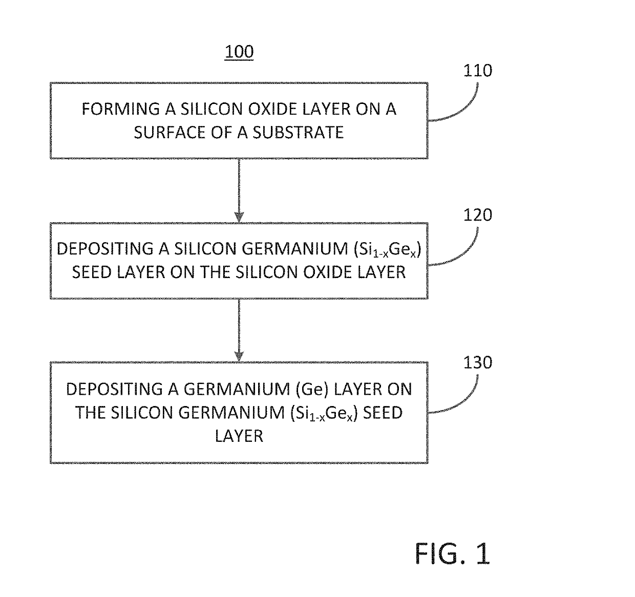
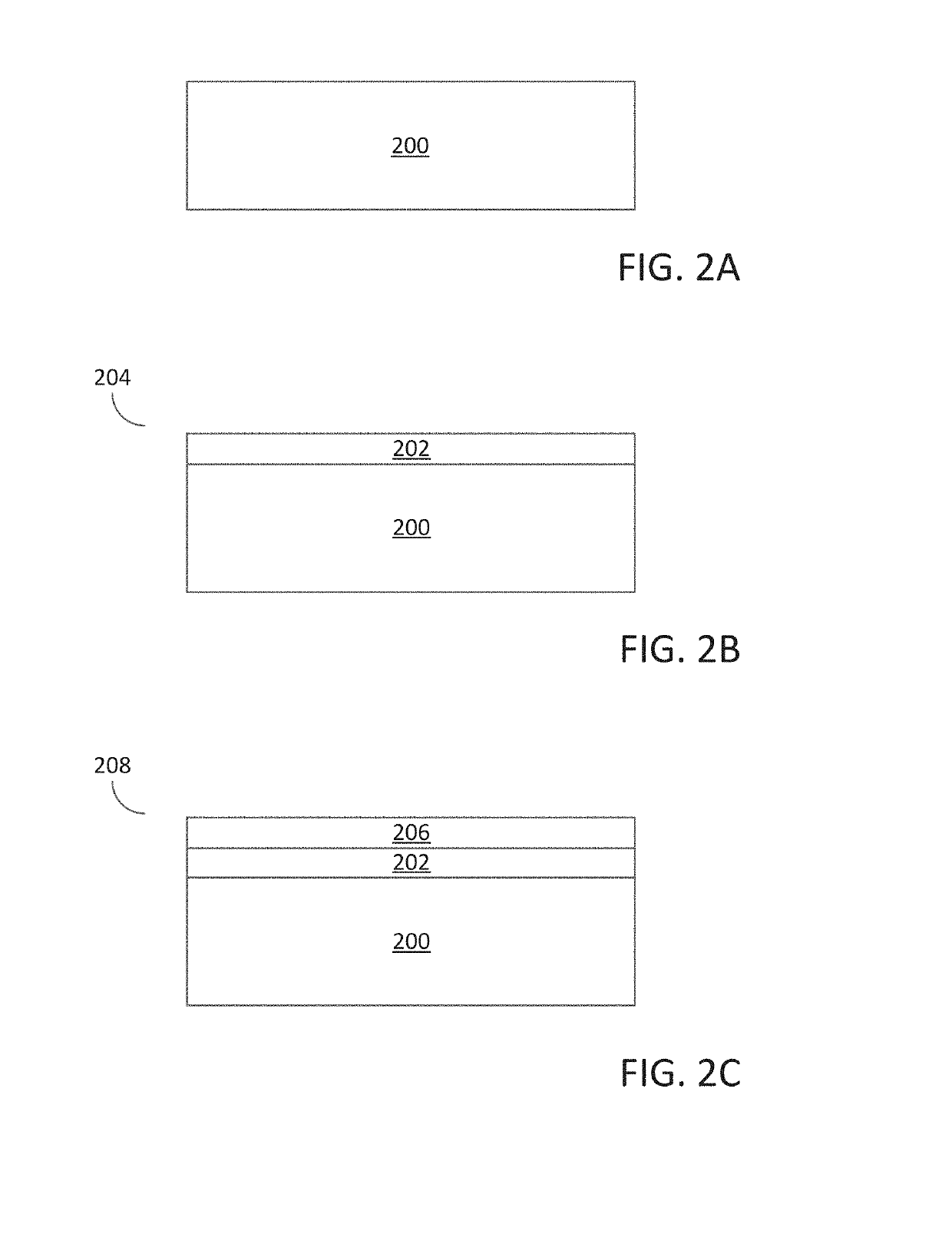
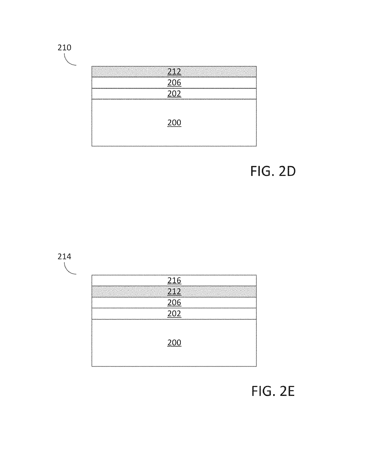
[0015]As used herein, the term “substrate” may refer to any underlying material or materials that may be used, or upon which, a device, a circuit or a film may be formed.

[0016]As used herein, the term “silicon germanium” and “Si1-xGex” may refer to an alloy of silicon and germanium, wherein the ratio of germanium to silicon may range as 1≥x≥0.

[0017]As used herein, the term “chemical vapor deposition” may refer to any process wherein a substrate is exposed to one or more volatile precursors, which react and / or decompose on a substrate surface to produce a desired deposition.

[0018]In the...


PUM


Abstract

A method for forming a forming a semiconductor structure is disclosed. The method may include: forming a silicon oxide layer on a surface of a substrate, depositing a silicon germanium (Si1-xGex) seed layer directly on the silicon oxide layer, and depositing a germanium (Ge) layer directly on the silicon germanium (Si1-xGex) seed layer. Semiconductor structures including a germanium (Ge) layer deposited on silicon oxide utilizing an intermediate silicon germanium (Si1-xGex) seed layer are also disclosed.

Description

FIELD OF INVENTION[0001]The present disclosure generally relates to methods for forming a semiconductor structure and particular to methods for depositing a germanium layer over a silicon oxide layer utilizing an intermediate silicon germanium (Si1-xGex) seed layer. The present disclosure also generally relates to semiconductor structures and particularly semiconductor structures including a germanium layer deposited over a silicon oxide layer utilizing an intermediate silicon germanium (Si1-xGex) seed layer.BACKGROUND OF THE DISCLOSURE[0002]As semiconductor devices continue to decrease in size in advanced technology nodes, a number of challenges arise in developing higher performance devices. One approach to increase the performance of semiconductor devices is to increase the carrier mobility, i.e., electrons and / or holes, in the channel region of the device. Although it is possible to obtain higher carrier mobilities with strained silicon, much higher mobilities may be achieved by...

Claims


Application Information

Patent Timeline
IPC IPC(8): H01L21/02H01L29/165
CPCH01L21/0245H01L29/165H01L21/02164H01L21/02532H01L21/02595H01L29/1054H01L21/02488H01L21/02502H01L21/0262H10B41/27H10B43/27
Inventor KOHEN, DAVIDPROFIJT, HARALD BENJAMINKRETZSCHMAR, ANDREW
Owner ASM IP HLDG BV
Why Eureka
Try Eureka