Light emitting device and method for manufacturing light emitting device

a technology manufacturing methods, which is applied in the field of light emitting devices, can solve the problems of obstructing the view of the iris, difficult mass production, and high cost, and achieve the effect of different optical refractive index

Active Publication Date: 2019-05-16
SHENZHEN RAYSEES AI TECH CO LTD
View PDF9 Cites 1 Cited by
  • Summary
  • Abstract
  • Description
  • Claims
  • Application Information

AI Technical Summary

Benefits of technology

[0008]In one embodiment, the sealed chamber is a vacuum chamber or contains air or special gas (e.g., dinitrogen, argon, inert gas). The sealed chamber has a different optical refractive index from the surrounding materials and is necessary to obtain the desired beam angle. It also helps to protect the light-emitting elements from being contaminated by dusts created during the cutting process of mass production. The light-emitting element used in the present invention may be an IR (infrared) LED or a LED producing any light wavelength. The light-emitting element may be a lateral, vertical or flip chip. Also, the light-emitting element may be a CSP (chip-scale package) chip, white chip, VCSEL (vertical-cavity surface-emitting laser) chip, or SLED (super luminescent diode) chip. Alternatively, the light-emitting element may also be a die array.
[0009]In addition, a method of manufacturing the light-emitting device is provided. The method includes providing a first sheet of molded structure comprising a plurality of molded bodies having metal leads; placing a second sheet of molded structure comprising a plurality of lenses on top of the first sheet of molded structure; bonding the first sheet of molded structure with the second sheet of molded structure to create a bonded structure so that each molded body forms a sealed chamber with a corresponding lens to enclose a light-emitting element; and cutting the bonded structure to create light emitting devices. As discussed above, the sealed chambers help to protect the light-emitting elements from being contaminated by dust created during the cutting process.

Problems solved by technology

Natural light often reflects off the iris, creating glare that can obstruct part of the view of the iris.
But they are expensive and difficult to make.
Such manufacturing process is complicated and difficult to scale for mass production.
However, such LED devices do not have light focusing lenses and therefore cannot be used as light sources for iris recognition systems.
Furthermore, the disclosed device's LED is already covered by a sealing member made from epoxy resin or similar polymer material, lenses made from such materials won't be effective in focusing light emitted from the LED.

Method used


Image

  • Light emitting device and method for manufacturing light emitting device
  • Light emitting device and method for manufacturing light emitting device
  • Light emitting device and method for manufacturing light emitting device

Examples


Embodiment Construction

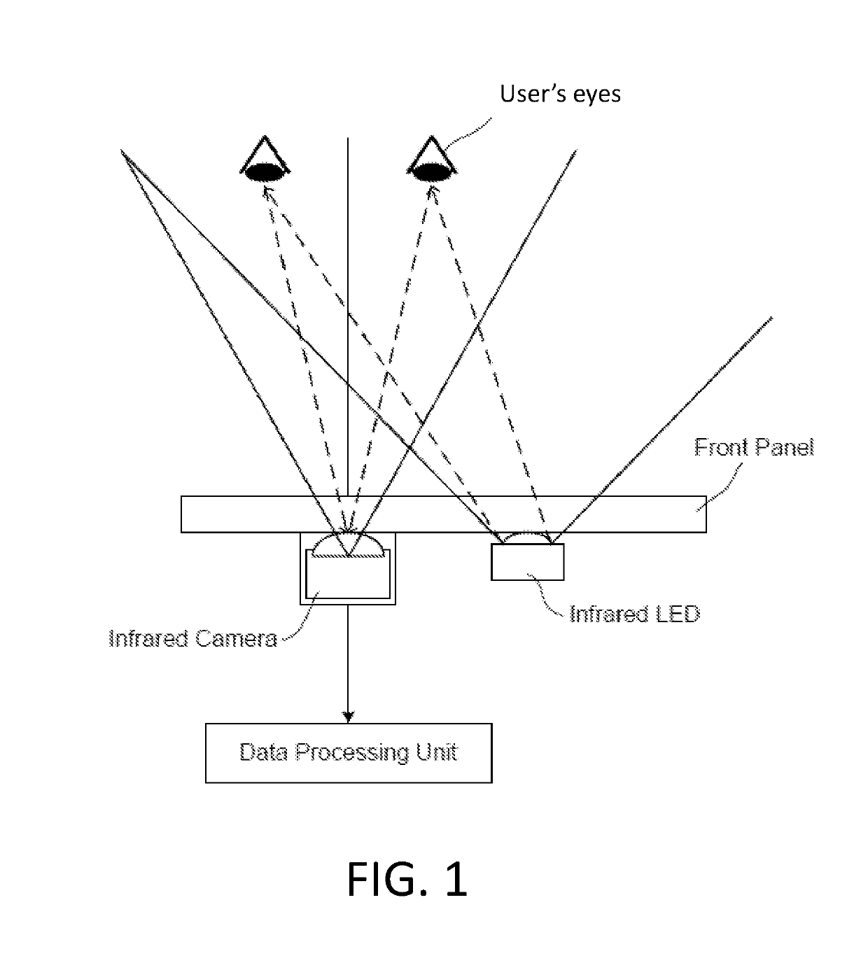
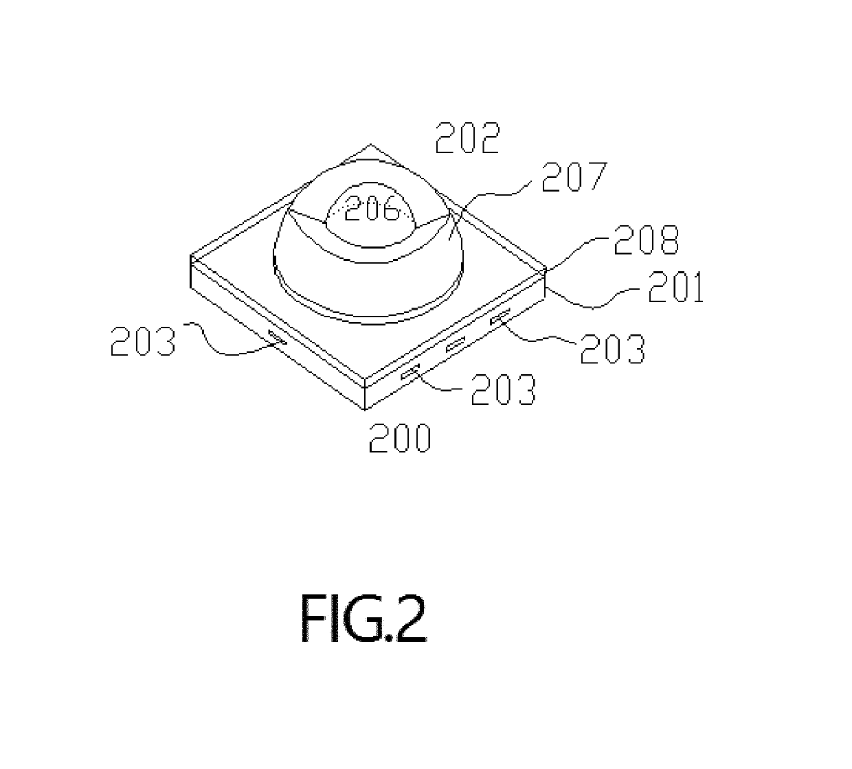
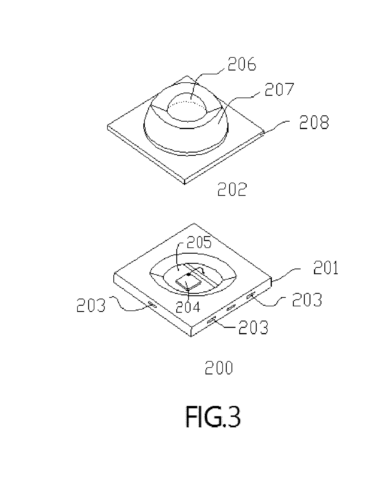
[0026]FIG. 2 is a three-dimensional illustration of an embodiment of a light-emitting device according to the invention. FIG. 3 is an exploded view of the embodiment shown in FIG. 2. FIG. 4A is a cross-sectional view of the embodiment shown in FIG. 2. As shown in these figures, the light-emitting device 200 includes a molded body 201 and a lens 202. The molded body 201 has raised edges that form a concave portion. At the bottom of the concave portion are metal leads 203, which extend to the outer edges of the molded body 201, and a plane surface 205. A light-emitting element 204 (e.g., a light-emitting diode) is mounted onto the plane surface 205 and is wire bonded to the metal leads 203 for receiving electric power.

[0027]The lens 202 includes a central portion 206, an edge portion 207 surrounding the central portion 206, and a base portion 208 supporting the central portion 206 and the edge portion 207. The central portion 206 is a dome-shaped structure symmetric across its central...


PUM


Abstract

A light-emitting device and a method of manufacturing the device are disclosed in this invention. The light-emitting device includes a molded body having metal leads and a plane surface for mounting a light-emitting element. The light-emitting device also includes a lens having one central portion, one edge portion surrounding the central portion, and one base portion supporting the central portion and the edge portion. The central portion has a dome-shaped top surface. The edge portion has one inner top surface and one outer top surface, and the inner top surface of the edge portion connects with the dome-shaped top surface of the central portion to form a valley-shaped groove. The base portion is attached onto the molded body to form a sealed chamber to enclose the light-emitting element.

Description

CROSS-REFERENCE TO RELATED APPLICATION[0001]This application is a divisional of and claims priority to U.S. patent application Ser. No. 15 / 588,688, filed May 7, 2017, the content of which is incorporated herein by reference in its entirety.FIELD OF INVENTION[0002]This invention generally relates to a light emitting device and to a method of manufacturing such a light emitting device.BACKGROUND OF THE INVENTION[0003]Iris biometrics is now considered one of the trilogy of the most important biometrics: face, fingerprint, and iris. The U.S. military is utilizing iris recognition to help prevent terrorism. Several nations around the world are in the process of creating National ID programs that will include all three of these biometrics. FIG. 1 is a schematic diagram illustrating an iris recognition system. As shown, a typical iris recognition system includes three key components: a light source, a camera unit, and a data processing unit. Natural light often reflects off the iris, creat...

Claims


Application Information

Patent Timeline
Patent Type & Authority Applications(United States)
IPC IPC(8): H01L33/54H01L33/56H01L33/48H01L33/62H01L33/58G06V10/145
CPCH01L33/54H01L33/56H01L33/486H01L33/62H01L33/58G06K9/00604H01L2933/0033H01L2933/005G06K9/2036H01L2933/0058H01L33/0058G06V40/19G06V10/145
Inventor WANG, YANG
Owner SHENZHEN RAYSEES AI TECH CO LTD
Why Eureka
Try Eureka