Circular photonic crystal structure, light emitting diode device and photoelectric conversion device

a technology light emitting diode, which is applied in the direction of instruments, optical elements, optical waveguide light guides, etc., can solve the problems of reducing the efficiency of light extraction and other types of photoelectric conversion device such as organic light emitting diodes or solar cells, so as to improve the light extraction efficiency of a photoelectric conversion device and improve the uniformity of light output of a light emitting device.

Active Publication Date: 2014-06-17
IND TECH RES INST
View PDF11 Cites 1 Cited by
  • Summary
  • Abstract
  • Description
  • Claims
  • Application Information

AI Technical Summary

Benefits of technology

[0008]A circular photonic crystal structure is applied in the present application to improve light extraction efficiency of a photoelectric conversion device. In addition, uniformity of light output of a light emitting device can be improved by applying the circular photonic crystal structure.
[0012]A photoelectric conversion device applying the aforementioned circular photonic crystal structure is provided. The photoelectric conversion device comprises a photoelectric conversion part, a first medium and the circular photonic crystal structure. The photoelectric conversion part is suitable for emitting or receiving a light. The first medium is located in a periphery of the photoelectric conversion part. The light passes through the first medium and a second medium outside the first medium, and the first medium and the second medium have different refractive indices. The circular photonic crystal structure is configured on a junction surface between the first medium and the second medium to improve light extraction efficiency of the photo electric conversion device.
[0013]A light emitting diode device applying the aforementioned circular photonic crystal structure is provided. The light emitting diode device comprises a substrate, a first-type doped semiconductor layer, a second-type doped semiconductor layer, an active region, a first electrode, a second electrode and the circular photonic crystal structure. The first-type doped semiconductor layer is disposed on the substrate. The second-type doped semiconductor layer is disposed on the first-type doped semiconductor layer. The active region is located between the first-type doped semiconductor layer and the second-type doped semiconductor layer. The first electrode is disposed on the first-type doped semiconductor layer, and then the second electrode is disposed on the top of device. Finally, the circular photonic crystal structure is fabricated on a top surface of the second-type doped semiconductor layer or between the first-type doped semiconductor layer and the substrate so as to improve light extraction efficiency of the light emitting diode device.

Problems solved by technology

However, an ordinary light emitting diode device suffers from total reflection between itself and an external medium, wherein a considerable quantity of light is restricted within the light emitting diode device and thereby the light extraction efficiency is lowered.
Similarly, efficiency of other types of photoelectric conversion device such as organic light emitting diodes or solar cells is also limited for the same reason as mentioned above.

Method used


Image

  • Circular photonic crystal structure, light emitting diode device and photoelectric conversion device
  • Circular photonic crystal structure, light emitting diode device and photoelectric conversion device
  • Circular photonic crystal structure, light emitting diode device and photoelectric conversion device

Examples


Embodiment Construction

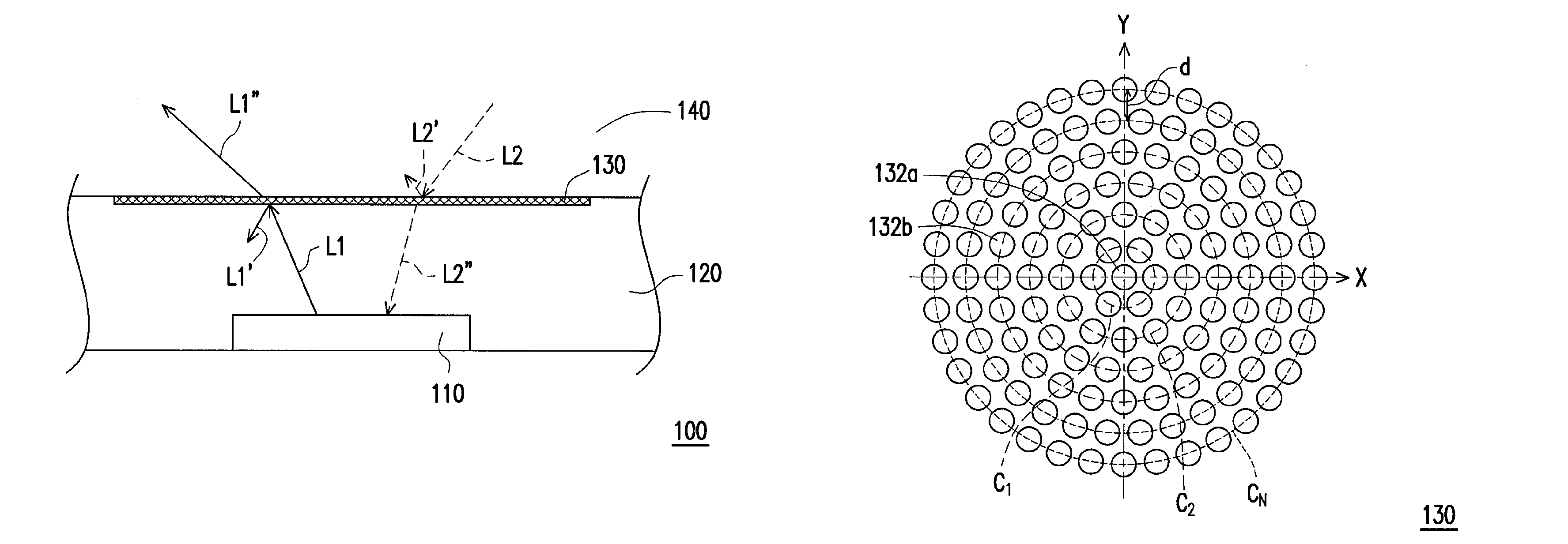
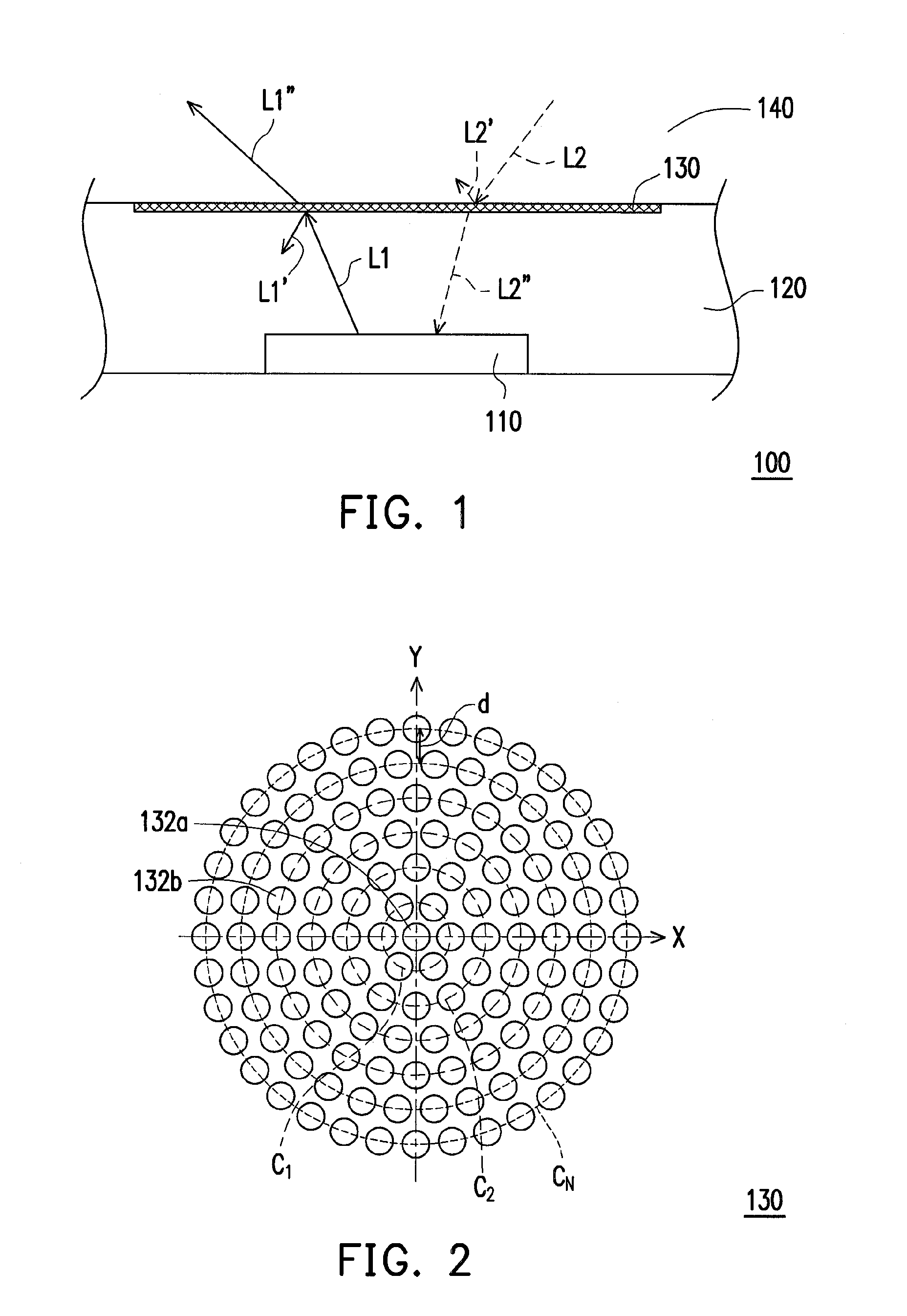
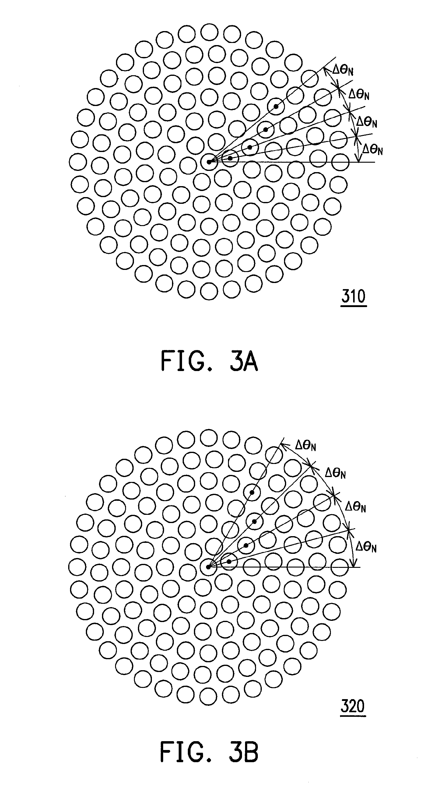
[0020]The circular photonic crystal is a kind of photonic quasi crystal having rotational symmetric structure. The total reflection on a surface of a medium can be reduced by forming the circular photonic crystal structure thereon such that most lights can be outputted from the medium or enter the medium. Furthermore, a photonic crystal structure has a photonic band gap (PBG) and provides guided mode and leaky mode, which improve light emitting efficiency and uniformity of light output. More particularly, as compared with a conventional photonic crystal structure, the circular photonic crystal structure of the present application has higher rotational symmetry, which conduces isotropic photonic band gap and is capable of improving the light extraction efficiency or optical properties of the photoelectric conversion device.

[0021]On the other hand, the circular photonic crystal structure of the present application can be defined by equations. The rotational symmetry of the circular ph...


PUM


Abstract

A method applying a circular photonic crystal structure to improve optical properties of a photoelectric conversion device such as a light emitting diode device, an organic light emitting diode device or a solar cell is provided, wherein the circular photonic crystal structure is configured on a junction surface between two different mediums where passes a light emitted or received by the photoelectric conversion device. The circular photonic crystal structure provides isotropic photonic band gap which conduces high light extraction efficiency.

Description

CROSS-REFERENCE TO RELATED APPLICATION[0001]This application claims the priority benefit of Taiwan application serial no. 100110580, filed Mar. 28, 2011. The entirety of the above-mentioned patent application is hereby incorporated by reference herein and made a part of this specification.BACKGROUND[0002]1. Technical Field[0003]The present application is related to a photoelectric conversion device having a circular photonic crystal structure.[0004]2. Description of Related Art[0005]Being advantaged in long life duration, superior color saturation, high response speed and stability etc., light emitting diodes (LEDs) are broadly used in the mainstream of new generation of illumination apparatus, such as traffic lights, backlight modules of liquid crystal displays, or high power output illumination apparatus.[0006]A light emitting efficiency of a light emitting diode depends on the external quantum efficiency thereof, while the external quantum efficiency of the light emitting diode i...

Claims


Application Information

Patent Timeline
Patent Type & Authority Patents(United States)
IPC IPC(8): G02B6/122
CPCG02B6/1225G02B1/005H01L31/0524H01L51/447B82Y20/00Y02E10/549Y02E10/52H01L51/5275H01L31/0543H10K30/87H10K50/858
Inventor HSU, CHIA-CHENLIN, JIAN-HUNGCHANG, TIEN-LILIN, HUNG-YICHOU, TA-HSINTSAI, JEN-HUI
Owner IND TECH RES INST
Why Eureka
Try Eureka