Programming NAND flash with improved robustness against dummy wl disturbance

a programming nand flash and robustness technology, applied in the field of flash memory, can solve the problems of dummy word lines becoming more likely, and dummy cell charge trapping, so as to reduce the boosted potential of the first dummy memory cell, reduce the disturbance, and weaken the associated hot carrier

Active Publication Date: 2019-05-23
MACRONIX INT CO LTD
View PDF1 Cites 16 Cited by
  • Summary
  • Abstract
  • Description
  • Claims
  • Application Information

AI Technical Summary

Benefits of technology

[0012]A two-step waveform applied to the first dummy memory cell as described herein, including the first voltage level during the first time interval lower than the second voltage level during the second time interval, can diminish the boosted potential of the first dummy memory cell during the first time interval, reduce the disturbance on the first dummy memory cell, and weaken the associated hot carrier effect.
[0013]The two-step waveform can also alleviate the erased state disturbance of an edge memory cell adjacent the first dummy memory cell, because the boosting efficiency of the edge memory cell is enhanced via the rise of the bias on the first dummy memory cell from the first voltage level (e.g. Vdwl-pre) to the second voltage level (e.g. Vdwl) in the second time interval. The boosting efficiency as used herein can be roughly expressed as the boosted channel potential of a specific word line divided by the applied bias to the specific word line.

Problems solved by technology

In cases without dummy word lines, the edge word lines for the NAND strings are more vulnerable to disturbance caused by Fowler-Nordheim (FN) tunneling or hot carrier effect since they are located in a place along a string of memory cells where the E-field can be high in some situations.
Nevertheless, now that multiple dummy word lines are located between GSL / SSL and the edge word lines, the dummy word lines become more likely to suffer hot carrier effects that can cause charge trapping in the dummy cells.
However, as the scaling of technology node continues and the need for multiple-bit per cell increases, the number of programming shots has increased drastically, which makes hot carrier effect and the associated disturbance almost inevitable for dummy word lines.
This issue is made even worse when considering that during a program operation on a selected NAND string, unselected NAND strings adjacent the selected NAND string undergo program inhibition.
Dummy memory cells are not addressable for purposes of data storage, and are not utilized to store data per se.

Method used


Image

  • Programming NAND flash with improved robustness against dummy wl disturbance
  • Programming NAND flash with improved robustness against dummy wl disturbance
  • Programming NAND flash with improved robustness against dummy wl disturbance

Examples


Embodiment Construction

[0033]The following description will typically be with reference to specific structural embodiments and methods. It is to be understood that there is no intention to limit the technology to the specifically disclosed embodiments and methods but that the technology may be practiced using other features, elements, methods and embodiments. Preferred embodiments are described to illustrate the present technology, not to limit its scope, which is defined by the claims. Those of ordinary skill in the art will recognize a variety of equivalent variations on the description that follows.

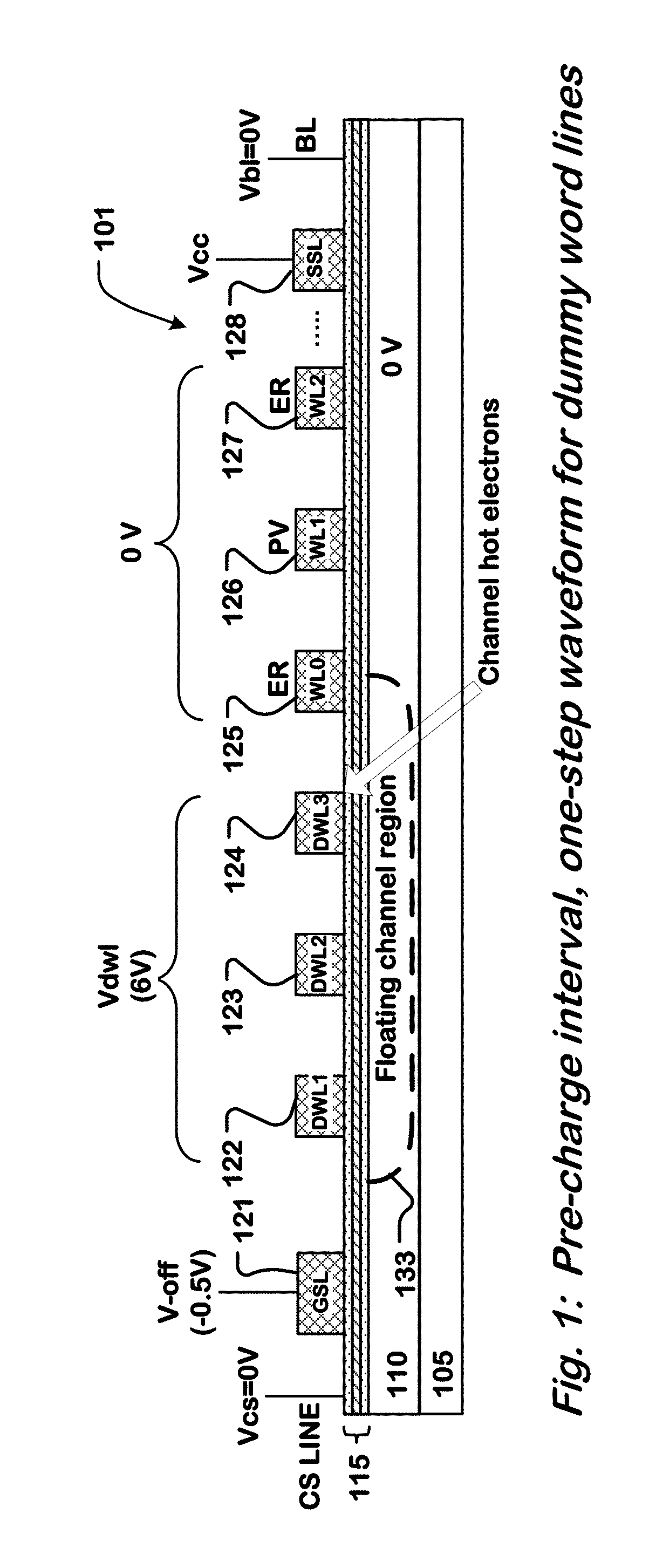
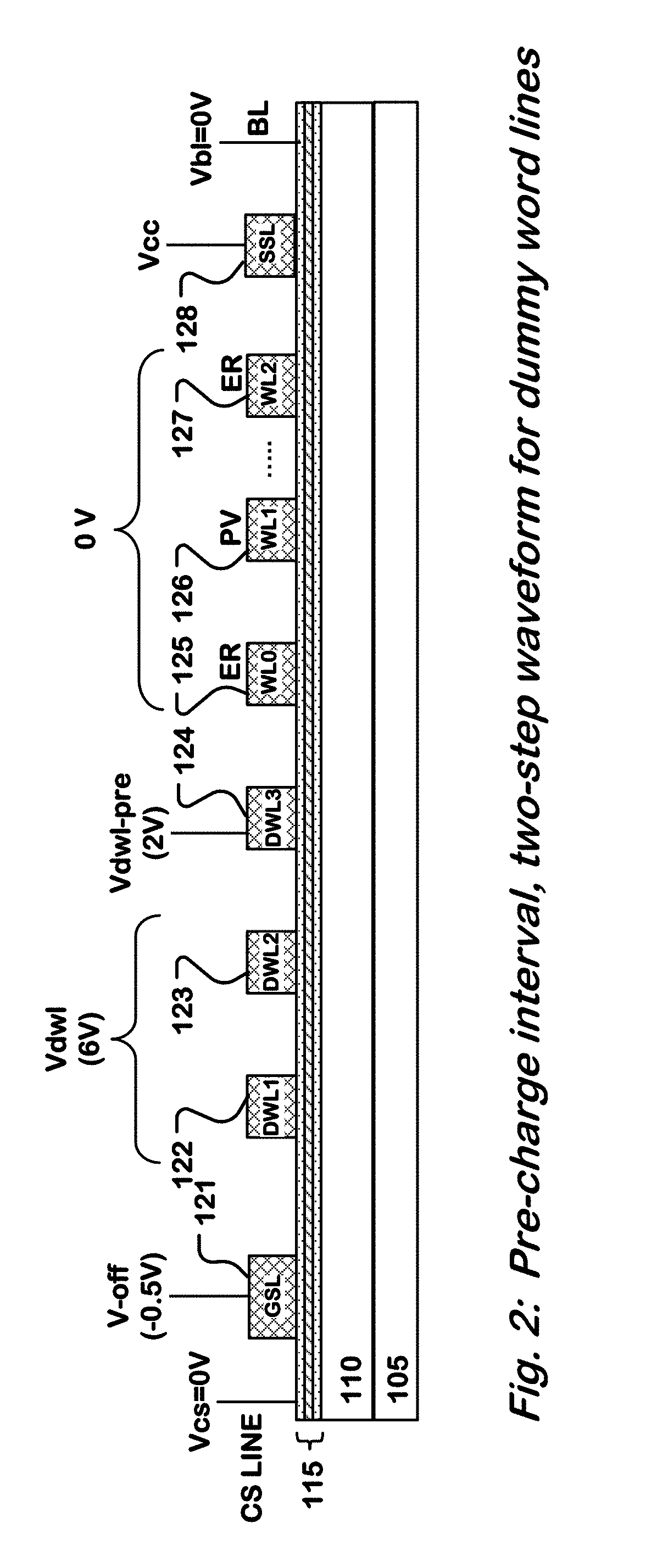
[0034]FIG. 1 is a simplified cross-sectional view of a memory device comprising a plurality of memory cells arranged in series in a semiconductor body (e.g. 105), such as can be applied for a NAND string (e.g. 101) in a NAND array. As shown in the example of FIG. 1, the NAND string is biased during a bit line pre-charge time interval, according to a programming method using a one-step waveform for dummy word...


PUM


Abstract

A memory device includes a plurality of memory cells arranged in series in a semiconductor body. First and second dummy memory cells arranged in series between a first string select switch and a first edge memory cell at a first end of the plurality of memory cells. The first dummy memory cell is adjacent the first edge memory cell, and the second dummy memory cell is adjacent the first string select switch. A channel line includes channels for the plurality of memory cells and the first and second dummy memory cells. Control circuitry is adapted for programming a selected memory cell in the plurality of memory cells corresponding to a selected word line by applying a switching voltage to the first dummy memory cell, the switching voltage having a first voltage level during a first time interval, and thereafter changing to a second voltage level higher than the first voltage level.

Description

BACKGROUNDField[0001]The present technology relates to flash memory, and more particularly to programming flash memory in a NAND configuration.Description of Related Art[0002]For both conventional 2D and 3D NAND Flash, dummy word lines have been used in the NAND strings for a variety of purposes. As the dimensions and density of the arrays have progressed, additional dummy word lines have been incorporated to alleviate the undesirable programming disturbance on edge word lines. In cases without dummy word lines, the edge word lines for the NAND strings are more vulnerable to disturbance caused by Fowler-Nordheim (FN) tunneling or hot carrier effect since they are located in a place along a string of memory cells where the E-field can be high in some situations.[0003]Nevertheless, now that multiple dummy word lines are located between GSL / SSL and the edge word lines, the dummy word lines become more likely to suffer hot carrier effects that can cause charge trapping in the dummy cell...

Claims


Application Information

Patent Timeline
Patent Type & Authority Applications(United States)
IPC IPC(8): G11C16/34G11C16/04G11C16/12G11C16/24
CPCG11C16/3427G11C16/0483H01L27/1157G11C16/24G11C16/12G11C16/08G11C16/10G11C16/105H10B41/35H10B43/35
Inventor CHEN, WEI-CHENLUE, HANG-TING
Owner MACRONIX INT CO LTD
Why Eureka
Try Eureka