Absorbance meter and semiconductor manufacturing device using absorbance meter

a technology of absorbance meter and semiconductor manufacturing device, which is applied in the direction of evaporator regulation/control, separation process, instruments, etc., can solve the problems of reducing measurement accuracy, reducing the distance between the light source and the light receiving part, and reducing the intensity of light received by the light receiving part. , to achieve the effect of increasing the distance from the light source part and keeping the measurement accuracy high

Inactive Publication Date: 2019-08-08
HORIBA STEC CO LTD
View PDF8 Cites 1 Cited by
  • Summary
  • Abstract
  • Description
  • Claims
  • Application Information

AI Technical Summary

Benefits of technology

[0020]According to the present invention configured as described above, even when measuring high-temperature sample gas, the need for increasing the distance from a light source part to a light receiving part is eliminated, and this enables measurement accuracy to be kept high.

Problems solved by technology

When trying to use the above-described conventional absorbance meter to measure such high temperature sample gas whose temperature is raised as high as 300° C. or more, it is necessary to considerably increase the thicknesses of the insulation parts in order to protect the light source part and the light receiving part from the heat of the sample gas, and along with this, the distance from the light source part to the light receiving part is also increased, so this causes the intensity of light received by the light receiving part to be reduced, thus reducing measurement accuracy.

Method used


Image

  • Absorbance meter and semiconductor manufacturing device using absorbance meter
  • Absorbance meter and semiconductor manufacturing device using absorbance meter
  • Absorbance meter and semiconductor manufacturing device using absorbance meter

Examples


Embodiment Construction

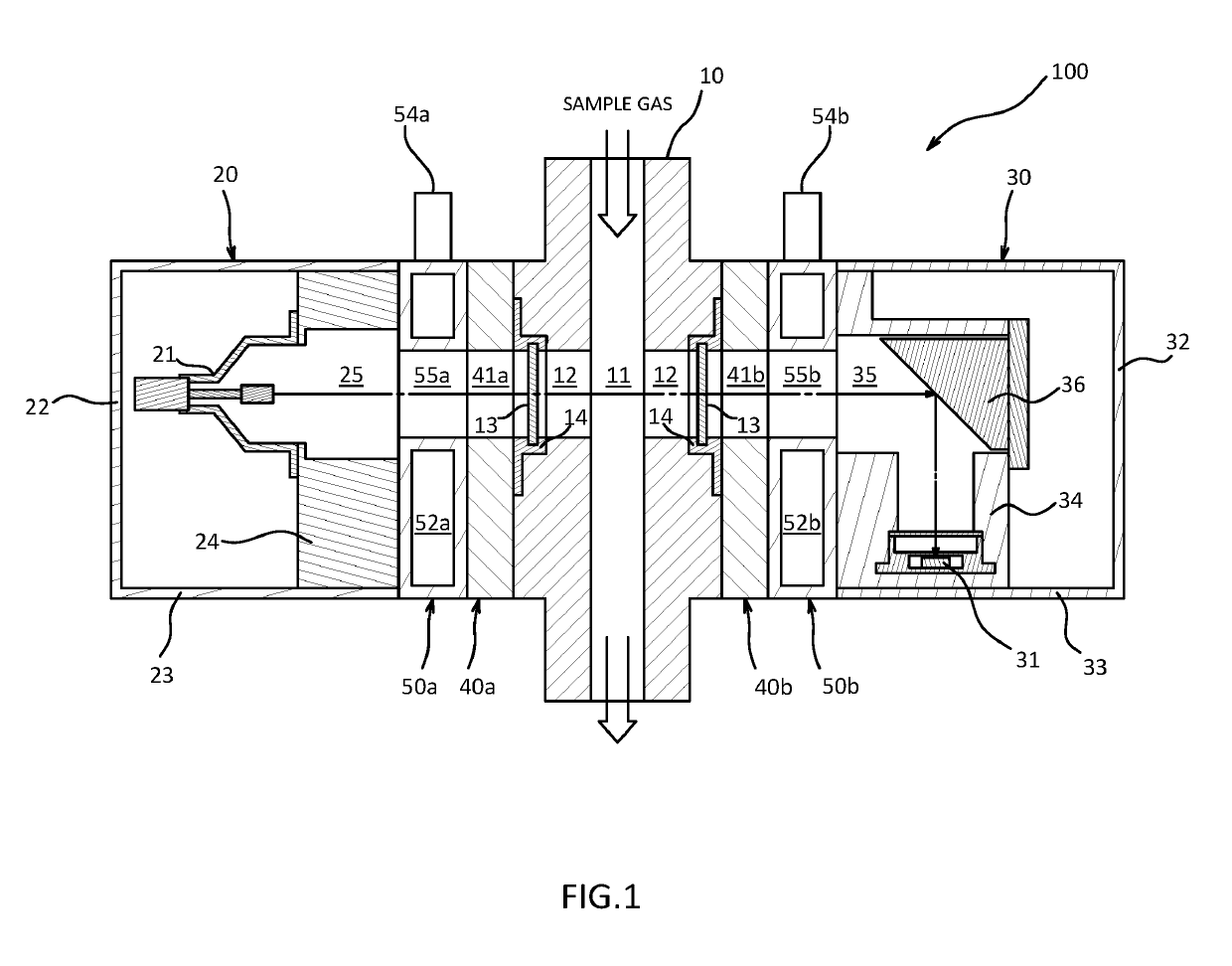
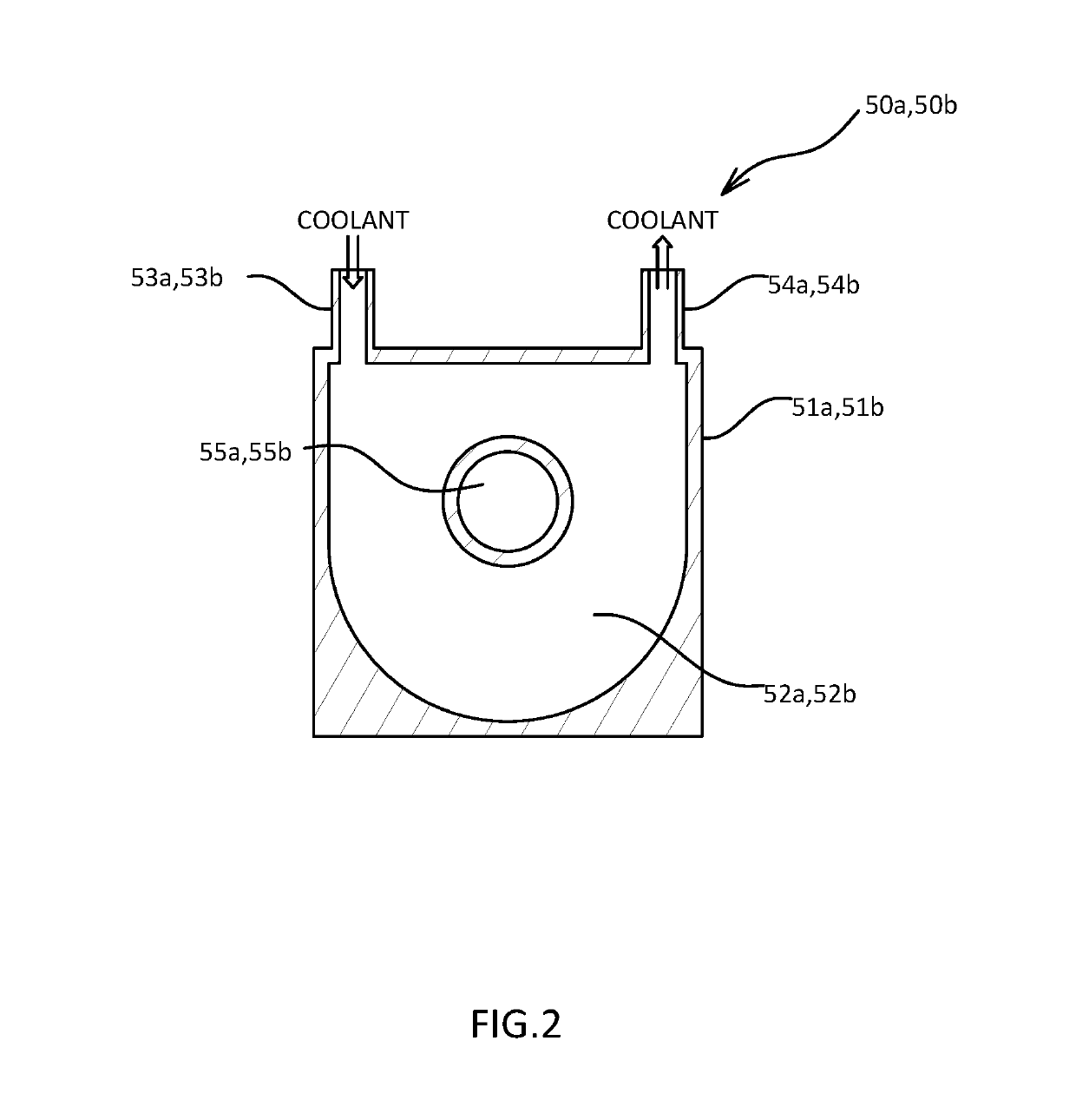
[0050]In the following, the absorbance meter according to the present invention will be described with reference to the drawings.

[0051]An absorbance meter 100 of the present embodiment is one using a so-called infrared spectroscopy (IR) that radiates infrared light having a predetermined wavelength to sample gas, and from the attenuation rate (transmittance) of it, measures the characteristics of a measurement target material contained in the sample gas. In addition, absorbance meters using the infrared spectroscopy include one using a Fourier transform infrared spectroscopy (FTIR) and one using a non-dispersive infrared analysis method (NDIR), and the present invention can also be applied to an absorbance meter using any of the infrared spectroscopies.

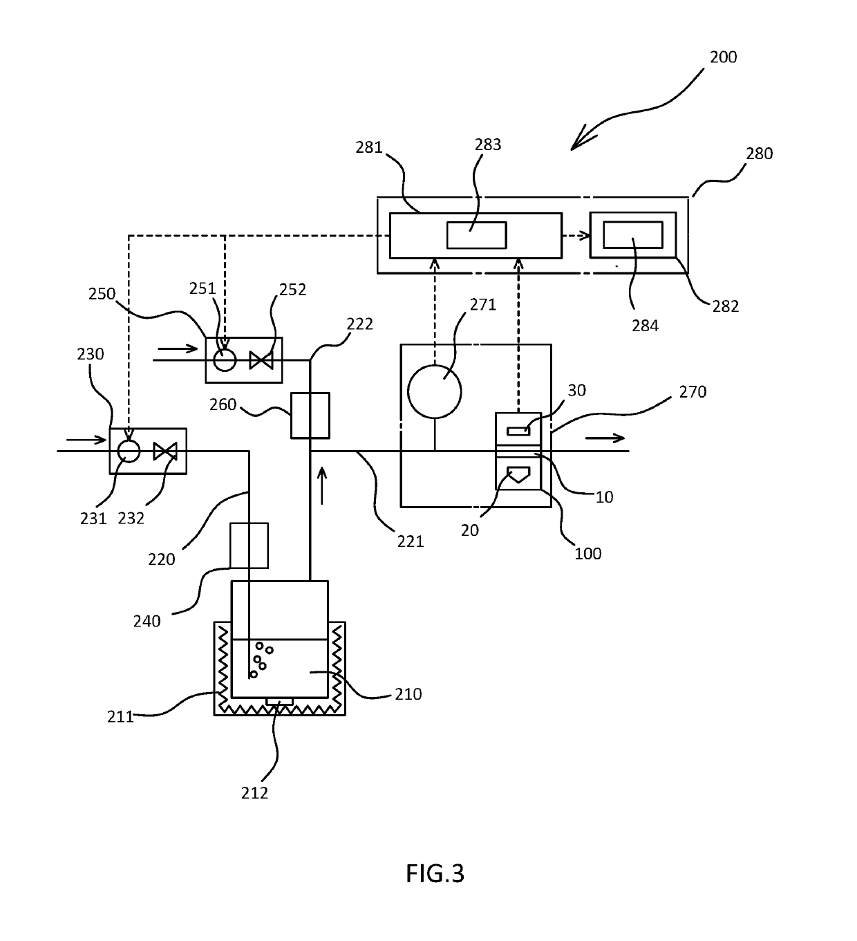
[0052]Also, the absorbance meter 100 of the present embodiment is used in a bubbling type semiconductor manufacturing device 200. Specifically, it is used when, in the bubbling type semiconductor manufacturing device 200, carrying mat...


PUM

PropertyMeasurementUnit
temperatureaaaaaaaaaa
absorbance meteraaaaaaaaaa
translucentaaaaaaaaaa

Abstract

Obtained is an absorbance meter capable of, when measuring high-temperature sample gas, without increasing the distance from a light source part to a light receiving part, protecting the light source part and the light receiving part from the heat of the sample gas and keeping measurement accuracy high. A sample accommodation part including an accommodation space for accommodating the sample gas, the light source part for radiating light into the accommodation space, the light receiving part for receiving light exiting from inside the accommodation space, a first insulation part disposed adjacent to the light source part side of the sample accommodation part, a second insulation part disposed adjacent to the light receiving part side of the sample accommodation part, a first cooling part disposed adjacent to the first insulation part, and a second cooling part disposed adjacent to the second insulation part are provided.

Description

TECHNICAL FIELD[0001]The present invention relates to an absorbance meter and a semiconductor manufacturing device using the absorbance meter.BACKGROUND ART[0002]As an absorbance meter using an infrared spectroscopy (IR) for measuring the concentration of sample gas, as disclosed in Patent Literature 1, there is one having: a sample accommodation part provided with a pair of translucent windows oppositely provided sandwiching an accommodation space for accommodating the sample gas; a light source part for radiating light into the accommodation space through a translucent window on one side; a light receiving part for receiving light passing through the accommodation space and existing from a translucent window on the other side; and insulation parts disposed adjacent to the light source part side and light receiving part side of the sample accommodation part and having through-holes facing the opposite translucent windows.[0003]In the above-described conventional absorbance meter, e...

Claims


Application Information

Patent Timeline
Patent Type & Authority Applications(United States)
IPC IPC(8): G01N21/61G01N1/38H01L21/67C23C16/52
CPCG01N21/61G01N1/38H01L21/67253C23C16/52H01L21/31G01N21/0332G01N21/05G01N21/3504G01N21/09C23C16/4482B01D1/14B01D1/0082G01N21/59
Inventor NISHIZATO, HIROSHIMINAMI, MASAKAZUSAKAGUCHI, YUHEI
Owner HORIBA STEC CO LTD
Why Eureka
Try Eureka