In-cell touch array substrate, display panel and manufacturing method thereof

a touch array substrate and in-cell technology, applied in the field of display techniques, can solve the problems of complex process and high cost, and achieve the effects of reducing the number of masks, reducing film formation, and simplifying the process

Inactive Publication Date: 2019-10-31
WUHAN CHINA STAR OPTOELECTRONICS TECH CO LTD
View PDF0 Cites 5 Cited by
  • Summary
  • Abstract
  • Description
  • Claims
  • Application Information

AI Technical Summary

Benefits of technology

[0021]The object of the present invention is to provide an in-cell touch array substrate, display panel and manufacturing method thereof to simplify the process and reduce the cost.
[0059]In summary, the in-cell touch array substrate, display panel and manufacturing method of the invention reduce the number of masks by one, reduce film-formation by three times, simplify process and reduce cost. The reduction of film-formation by three times, simplification of film structure, and avoidance of the three non-metal films of first insulation layer, second insulating layer and passivation layer from directly contacting the conductive film, thereby reduce the probability of film breakage due to poor stress matching, and reduce the high risk of undercutting when dry etching passivation layer to penetrate the three-layer films of passivation layer / second insulating layer / first insulating layer.

Problems solved by technology

A total of 14 mask processes are required to complete the process, and the process is complicated and costly.

Method used


Image

  • In-cell touch array substrate, display panel and manufacturing method thereof
  • In-cell touch array substrate, display panel and manufacturing method thereof

Examples


Embodiment Construction

[0063]To further explain the technique means and effect of the present invention, the following uses preferred embodiments and drawings for detailed description.

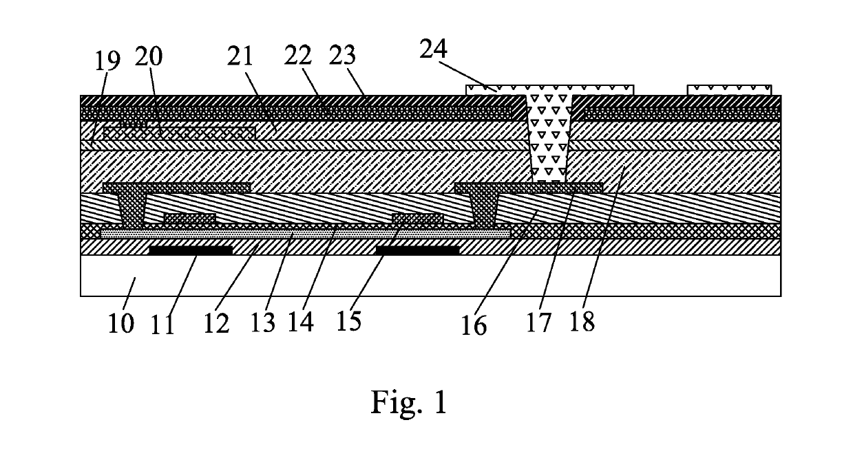
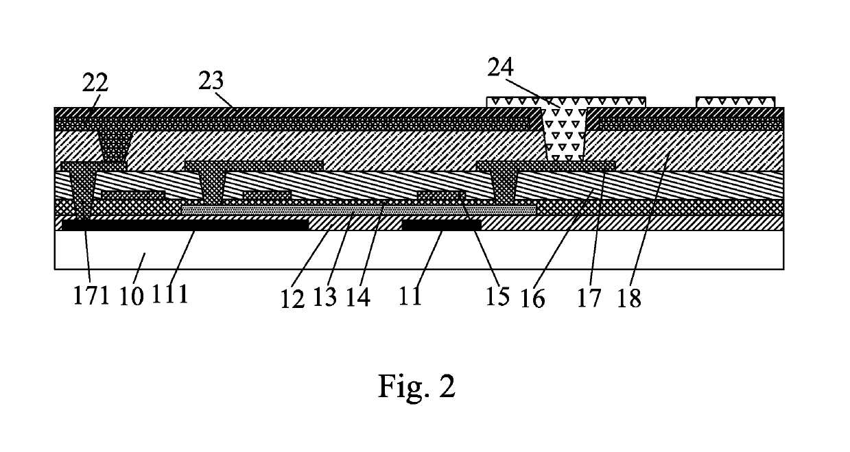
[0064]Referring to FIG. 2, FIG. 2 is a schematic view cross-sectional showing the in-cell touch array substrate of a preferred embodiment of the present invention. The in-cell touch array substrate of the preferred embodiment mainly comprises: a substrate 10; a LTPS TFT array disposed on the substrate 10, the LTPS TFT array comprising a patterned light-shielding layer 11 and a patterned source / drain layer 17; a patterned planarization layer 18 disposed on the LTPS TFT array; a patterned bottom transparent electrode (BITO) 22 disposed on the planarization layer 18, used as a touch signal electrode; a patterned passivation layer 23 disposed on the BITO 22; a patterned top transparent electrode (TITO) 24 disposed on the passivation layer 23, used as a pixel electrode.

[0065]In the present invention, the metal of source / drain lay...


PUM

PropertyMeasurementUnit
temperatureaaaaaaaaaa
shieldingaaaaaaaaaa
light-shieldingaaaaaaaaaa

Abstract

The invention provides an in-cell touch array substrate, a display panel and a manufacturing method thereof. The in-cell touch array substrate comprises: a substrate (10); an LTPS TFT array disposed on the substrate (10), comprising a patterned light-shielding layer (11) and a patterned source / drain layer (17); a patterned planarization layer (18) disposed on the LTPS TFT array; a patterned BITO (22) disposed on the planarization layer (18); and a patterned passivation layer (23) on BITO (22); a patterned TITO (24) disposed on the passivation layer (23); and a source / drain layer (17) comprising a first wire (171) connected to the upper BITO (22), the light-shielding layer (11) comprising a second wire (111) as a touch signal line, and the second wire (111) is connected to the upper first wire (171). The invention reduces one mask, reduces film-formation by three, simplifies the process and reduces the cost.

Description

BACKGROUND OF THE INVENTION1. Field of the Invention[0001]The present invention relates to the field of display techniques, and in particular to an in-cell touch array substrate, display panel and manufacturing method thereof.2. The Related Arts[0002]The touch display panel can be divided according to the structure: the touch circuit covering on the liquid crystal (LC) cell (On-Cell), the touch circuit embedded in the LC cell (In-Cell), and the external type. The in-cell touch display panel has the advantages of low cost and thinness, is favored by major panel manufacturers, and has evolved into the development mainstream of the future touch technology.[0003]Referring to FIG. 1, FIG. 1 is a schematic cross-sectional view of a conventional in-cell touch array substrate. At present, the high-resolution in-cell touch LCD has become the mainstream of low-temperature polysilicon (LTPS) LCD display panels. At present, the in-cell touch adopts the bottom transparent electrode (BITO) 22 as ...

Claims


Application Information

Patent Timeline
Patent Type & Authority Applications(United States)
IPC IPC(8): H01L27/12G02F1/1333G02F1/1362G02F1/1368G06F3/041
CPCG02F1/13338G02F2202/104H01L27/1248G02F1/136286G02F2001/136295G06F3/0412G06F2203/04103G02F1/136227H01L27/1259G02F2001/13685G02F1/136209H01L27/124G02F1/1368G06F3/04164G06F3/0443G02F1/136231H01L27/1255H01L29/66757H01L29/78633H01L29/78675G02F1/136295G02F1/13685
Inventor WANG, WEI
Owner WUHAN CHINA STAR OPTOELECTRONICS TECH CO LTD
Why Eureka
Try Eureka