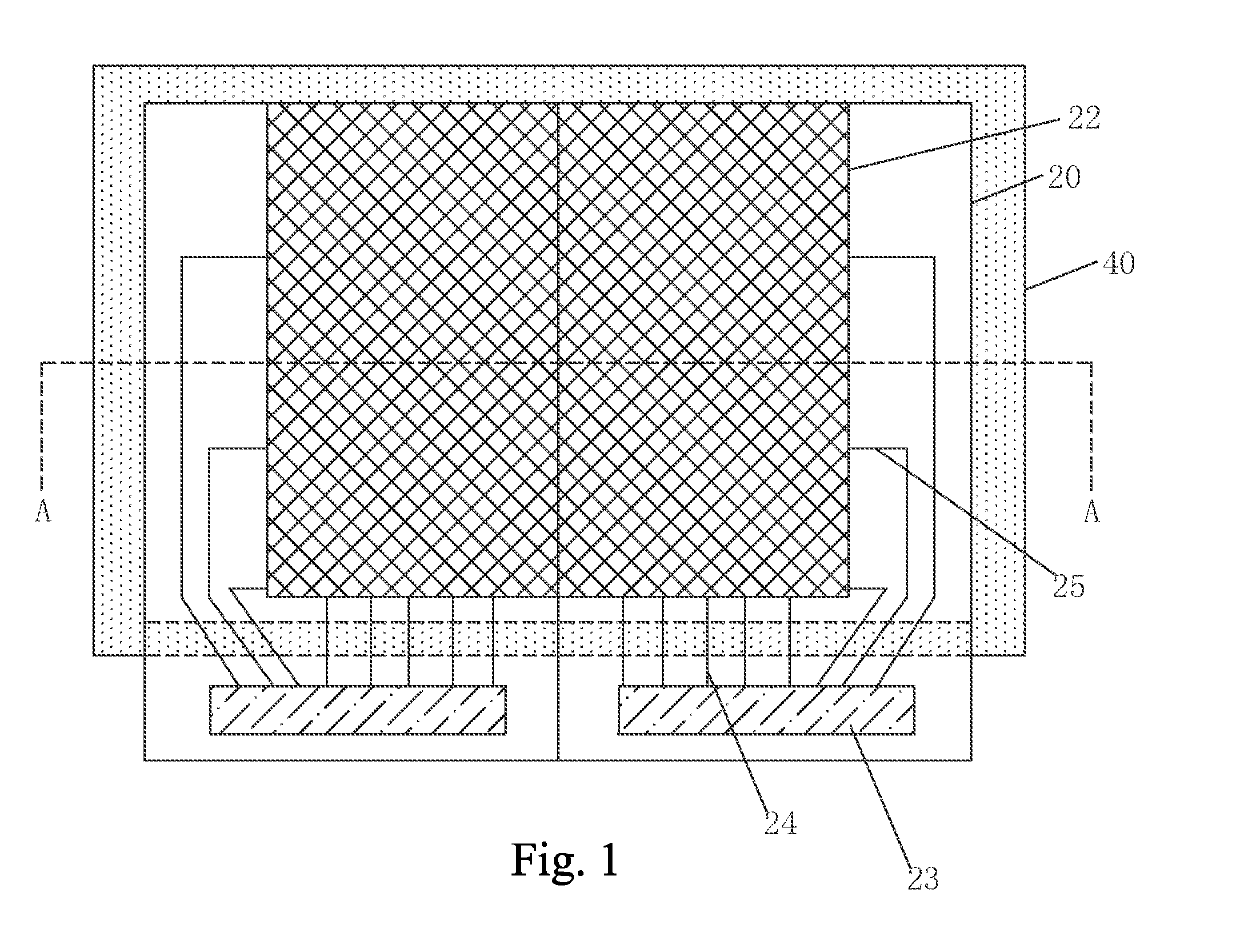
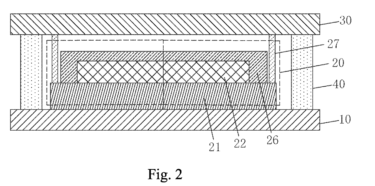
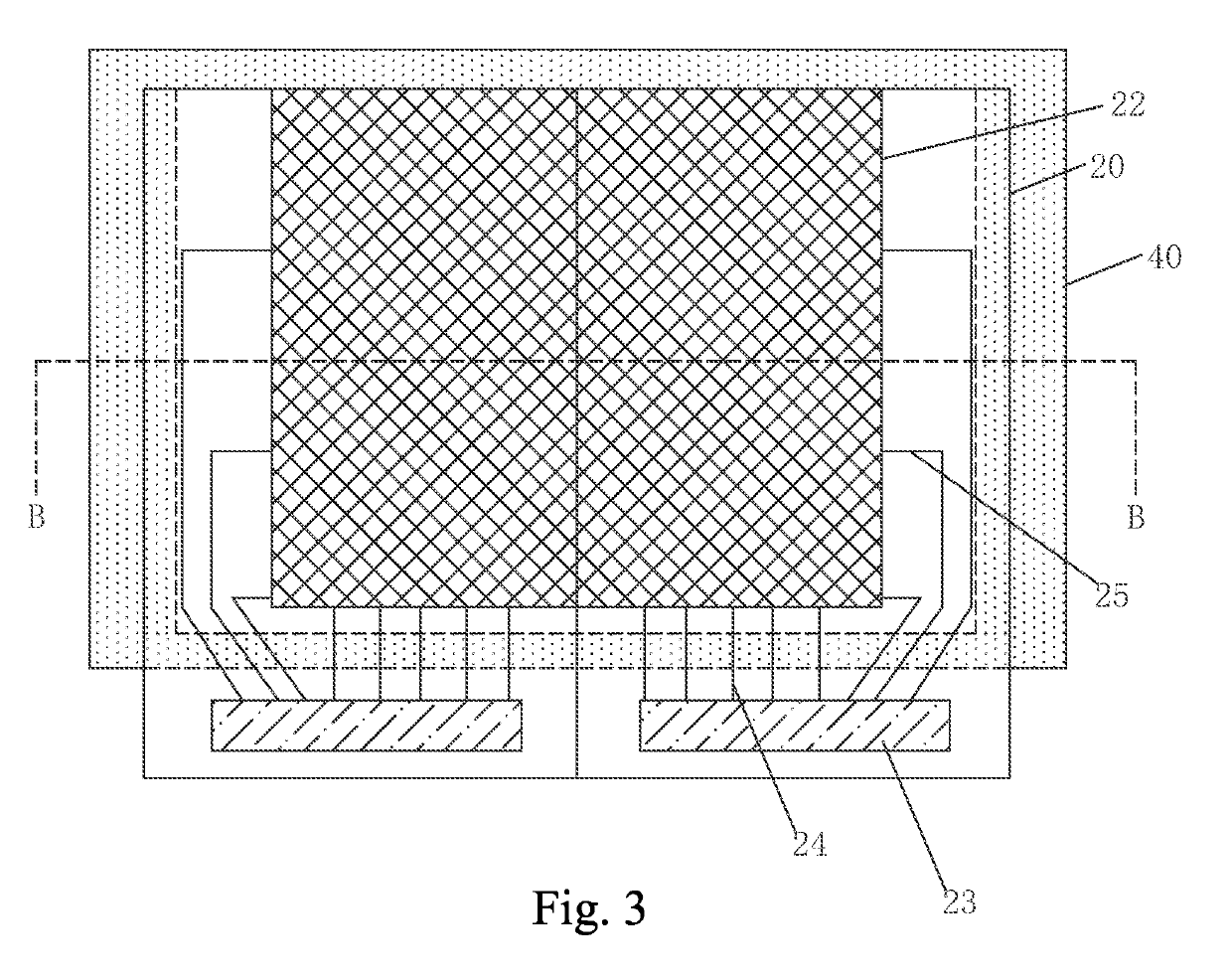
OLED display device

a display device and oled technology, applied in the field of display, can solve the problems of difficult to completely eliminate the splicing seam gap at the splicing seam of a plurality of oled display devices, difficult to manufacture known large-scale oled display devices, and suffer screen segmentation, etc., to improve the display quality reduce the segmentation sense of the oled display device, and reduce the gap

Inactive Publication Date: 2019-10-31
WUHAN CHINA STAR OPTOELECTRONICS TECH CO LTD
View PDF8 Cites 1 Cited by
  • Summary
  • Abstract
  • Description
  • Claims
  • Application Information

AI Technical Summary

Benefits of technology

[0017]The present invention provides the following advantages: the OLED display device of the present invention comprises: which comprises: a lower package layer, at least two adjacent OLED display units disposed on the lower package layer, and an upper package layer disposed on the at least two adjacent OLED display units; each OLED display unit comprising a substrate disposed on the lower package layer and a light-emitting layer disposed on the substrate. The at least two adjacent OLED display units are integrally package by the lower and the upper package layers. Therefore, a packaging structure for each OLED display unit is not necessary, so that the light-emitting layer in the adjacent OLED display unit of the present invention achieves seamless docking, which reduces the segmentation sense of the OLED display device, and reduces the gap between adjacent OLED display units and the light-emitting layers as well as improves the display quality of the OLED display device.

Problems solved by technology

The known large-scale OLED display devices are difficult to manufacture.
However, the splicing gaps at the splicing seams of a plurality of OLED display devices are difficult to completely eliminate in prior art, and the displayed image will suffer a screen segmentation.
Therefore, the gaps of the splicing OLED display device may become more pronounced because of the larger width of the package border.

Method used


Image

  • OLED display device
  • OLED display device
  • OLED display device

Examples


Embodiment Construction

[0025]To further explain the technical means and effect of the present invention, the following refers to embodiments and drawings for detailed description. Apparently, the described embodiments are merely some embodiments of the present invention, instead of all embodiments. All other embodiments based on embodiments in the present invention and obtained by those skilled in the art without departing from the creative work of the present invention are within the scope of the present invention.

[0026]The terms “comprising” and “having” and any variations thereof appearing in the specification, claims, and drawings of the present application are intended to cover non-exclusive inclusion. For example, a process, method, system, product, or device that includes a series of steps or units is not limited to the listed steps or units, but optionally also includes steps or units not listed, or alternatively, other steps or units inherent to these processes, methods, products or equipment. In...


PUM


Abstract

The invention provides an OLED display device, comprising: a lower package layer, at least two adjacent OLED display units disposed on the lower package layer, and an upper package layer disposed on the at least two adjacent OLED display units; each OLED display unit comprising a substrate disposed on the lower package layer and a light-emitting layer disposed on the substrate. The at least two adjacent OLED display units are integrally package by the lower and the upper package layers. Therefore, a packaging structure for each OLED display unit is not necessary, so that the light-emitting layer in the adjacent OLED display unit of the present invention achieves seamless docking, which reduces the segmentation sense of the OLED display device, and reduces the gap between adjacent OLED display units and the light-emitting layers as well as improves the display quality of the OLED display device.

Description

BACKGROUND OF THE INVENTION1. Field of the Invention[0001]The present invention relates to the field of display and, in particular, to the field of an OLED display device.2. The Related Arts[0002]The organic light-emitting diode (OLED) display, also known as organic electroluminescent display, is a new type of flat panel display device. Because of the advantages of self-emission, low driving voltage, high luminous efficiency, short response time, high definition and contrast, near 180° viewing angle, and wide operating temperature range, ability to realize flexible display and large-area full-color display, the OLED display device is recognized by the industry as the most promising display device.[0003]The OLED element generally comprises: a substrate, an anode disposed on the substrate, a hole injection layer disposed on the anode, a hole transport layer disposed on the hole injection layer, a light-emitting layer disposed on the hole transport layer, an electron transport layer di...

Claims


Application Information

Patent Timeline
Patent Type & Authority Applications(United States)
IPC IPC(8): H01L51/52H01L51/50
CPCH01L51/5012H01L51/5246H10K59/86H10K59/131H10K50/18H10K50/846H10K50/8426H10K2102/351H10K50/11H10K59/18H10K59/90
Inventor LI, XUEYUNTANG, YUEJUN
Owner WUHAN CHINA STAR OPTOELECTRONICS TECH CO LTD
Why Eureka
Try Eureka