

Light receiving element, imaging element, and imaging device
a technology of light receiving element and imaging element, which is applied in the direction of radiation control device, distance measurement, instruments, etc., can solve the problems of inability to ensure a sufficient photoelectric conversion region, limited photoelectric conversion region, and difficulty in obtaining a capd sensor having sufficient characteristics, etc., to achieve the effect of improving characteristics
- Summary
- Abstract
- Description
- Claims
- Application Information
AI Technical Summary
Benefits of technology
Problems solved by technology
Method used
Image

Examples
first embodiment
[0115]
[0116]The present technology is intended to improve characteristics such as a pixel sensitivity by a CAPD sensor having a rear surface irradiation type configuration.
[0117]The present technology, for example, can be applied to a solid-state imaging element configuring a distance measuring system measuring a distance by an indirect ToF method, an imaging device including such a solid-state imaging element, or the like.
[0118]For example, the distance measuring system is mounted on a vehicle, and can be applied to an in-vehicle system that measures a distance to a target outside the vehicle, a gesture recognition system that measures a distance to a target such as the hand of a user, and recognizes a gesture of the user on the basis of a measurement result, or the like. In this case, a gesture recognition result, for example, can be used for manipulating a car navigation system, or the like.
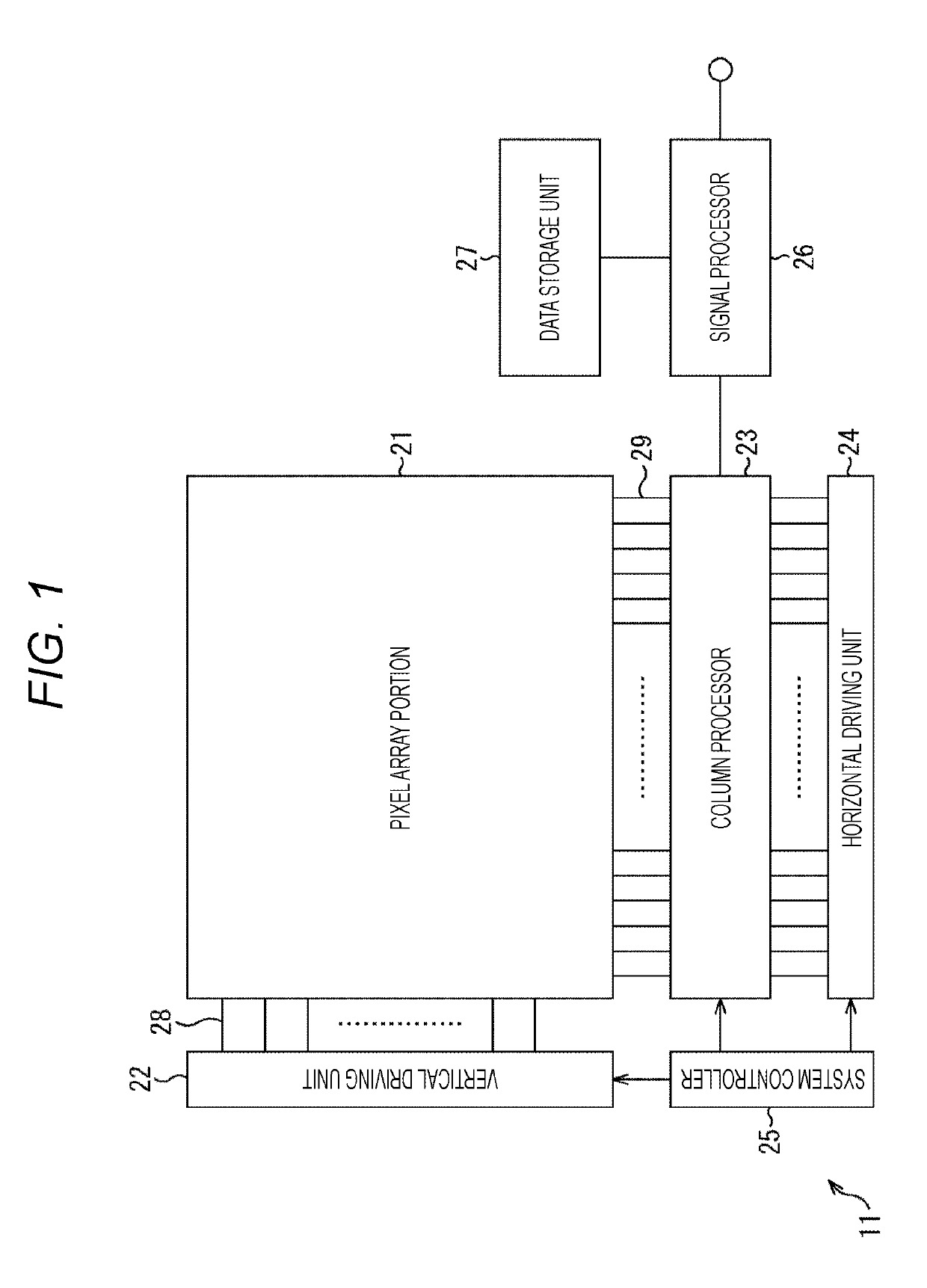
[0119]FIG. 1 is a diagram illustrating a configuration example of one embodiment of a soli...
modification example 1 of first embodiment
[0232]
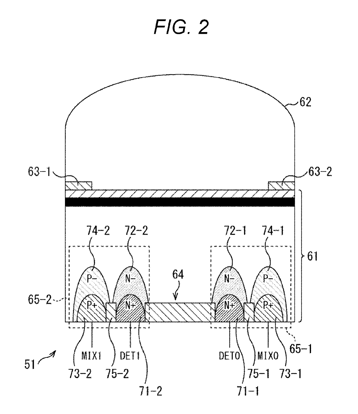
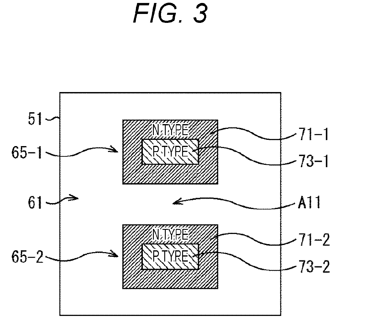
[0233]Furthermore, in the above description, as illustrated in FIG. 3, a case where the portion of the signal extraction unit 65 in the substrate 61 is a region in which the N+ semiconductor region 71 and the P+ semiconductor region 73 are in the shape of a rectangle, has been described as an example. However, the shape of the N+ semiconductor region 71 and the P+ semiconductor region 73 at the time of being seen from the direction vertical to the substrate 61 may be any shape.
[0234]Specifically, for example, as illustrated in FIG. 9, the N+ semiconductor region 71 and the P+ semiconductor region 73 may be in the shape of a circle. Furthermore, in FIG. 9, the same reference numerals will be applied to portions corresponding to those in FIG. 3, and the description thereof will be suitably omitted.
[0235]FIG. 9 illustrates the N+ semiconductor region 71 and the P+ semiconductor region 73 when the portion of the signal extraction unit 65 in the pixel 51 is seen from the direction ...
modification example 2 of first embodiment
[0241]
[0242]FIG. 11 is a plan view illustrating a modification example of a planar shape of the signal extraction unit 65 in the pixel 51.
[0243]The planar shape of the signal extraction unit 65, for example, may be an octagonal shape illustrated in FIG. 11, in addition to the rectangular shape illustrated in FIG. 3 and the circular shape illustrated in FIG. 7.
[0244]In addition, FIG. 11 illustrates a plan view in a case where the separation portion 75 including the oxide film or the like, is formed between the N+ semiconductor region 71 and the P+ semiconductor region 73.
[0245]In FIG. 11, line A-A′ indicates a sectional line in FIG. 37 as described later, and line B-B′ indicates a sectional line in FIG. 36 as described later.
PUM
 Abstract
Description
Claims
Application Information