Micro-led module and method for fabricating the same

a micro-led module and micro-led chip technology, applied in the direction of final product manufacturing, sustainable manufacturing/processing, semiconductor/solid-state device details, etc., can solve the problems of difficult to precisely mount the micro-led chips in their correct positions on the circuit board, and poor so as to improve the flatness of the circuit board and ensure the correct mounting of the micro-led chips.

Active Publication Date: 2019-11-28
LUMENS
View PDF0 Cites 19 Cited by
  • Summary
  • Abstract
  • Description
  • Claims
  • Application Information

AI Technical Summary

Benefits of technology

[0028]According to the prior art method, driver ICs are first attached to a circuit board with poor flatness and micro-LED chips are then mounted on the opposite surface of the circuit board. The attachment of the driver ICs further deteriorates the flatness of the circuit board, making it difficult to mount the micro-LED chips in correct positions. In contrast, according to the method of the present invention, micro-LED chips are first mounted on one surface of a circuit board whose flatness has been previously enhanced, and driver ICs are then attached to the opposite surface of the circuit board. The method of the present invention ensures precise and accurate mounting of the micro-LED chips on the circuit board.

Problems solved by technology

According to the conventional method, the circuit board has poor flatness, making it difficult to precisely mount the micro-LED chips in their correct positions on the circuit board.
Particularly, when the micro-LED chips are simultaneously attached to the surface of the circuit board by a multi-chip transfer process, poor flatness of the circuit board leads to severe defects, for example, a large difference in pitch between the micro-LED chips.
The circuit board is susceptible to natural deformation such as warpage, losing its flatness.
The micro-LED chips are difficult to attach to correct positions on the circuit board with poor flatness when mounted (particularly by a multi-chip transfer process).
However, when small-sized micro-LED chips are picked up from their original locations, placed in desired positions on a circuit board, and bonded to the circuit board, their small size makes it difficult to precisely control the pick-up and placing.
Due to this difficulty, the LED chips may not be seated in their correct positions or may be tilted, causing the formation of defects in a final display and deteriorating the reliability of the display.

Method used


Image

  • Micro-led module and method for fabricating the same
  • Micro-led module and method for fabricating the same
  • Micro-led module and method for fabricating the same

Examples


Embodiment Construction

[0037]Preferred embodiments of the present invention will now be described with reference to the accompanying drawings. It should be noted that the drawings and embodiments are simplified and illustrated such that those skilled in the art can readily understand the present invention.

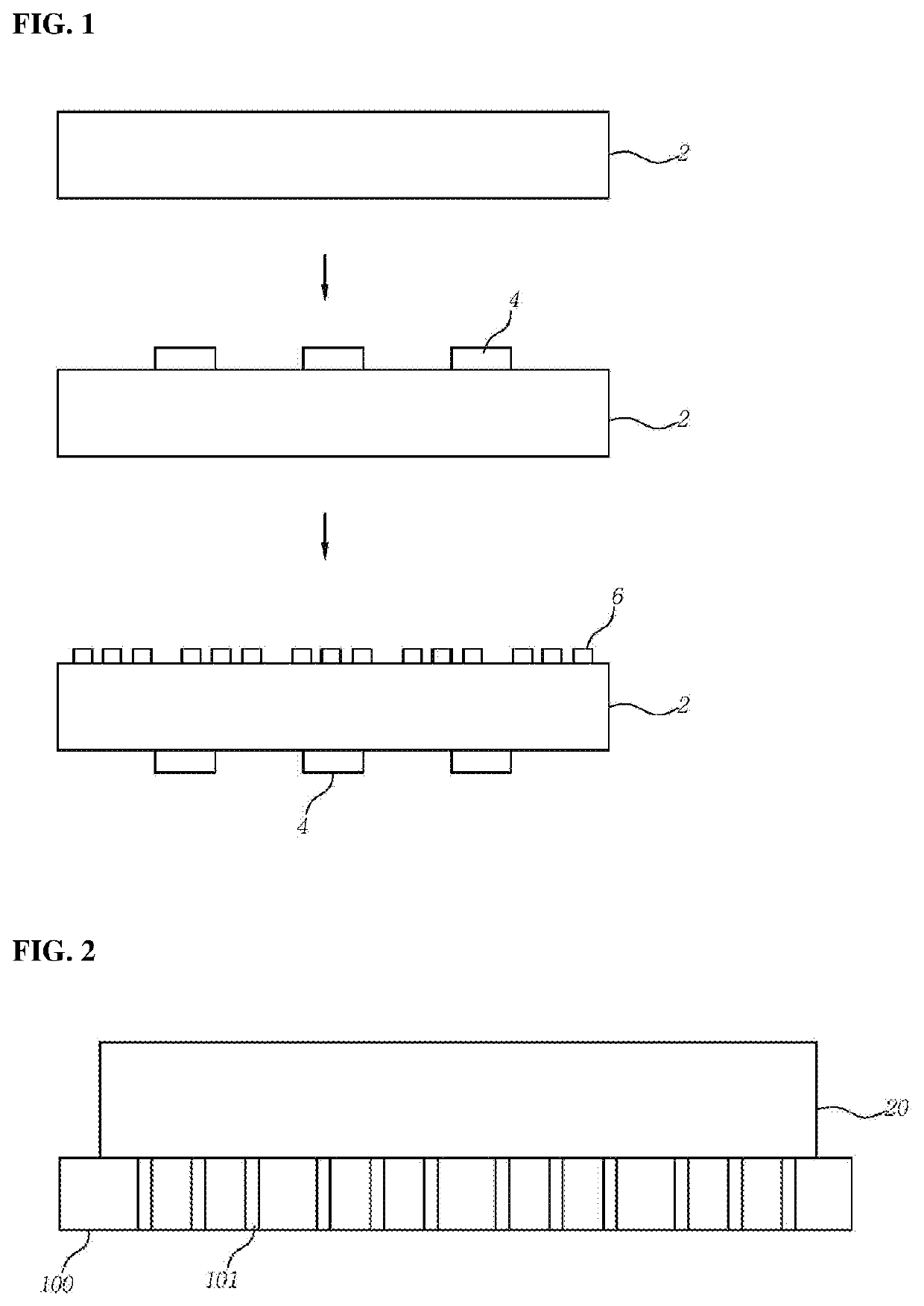
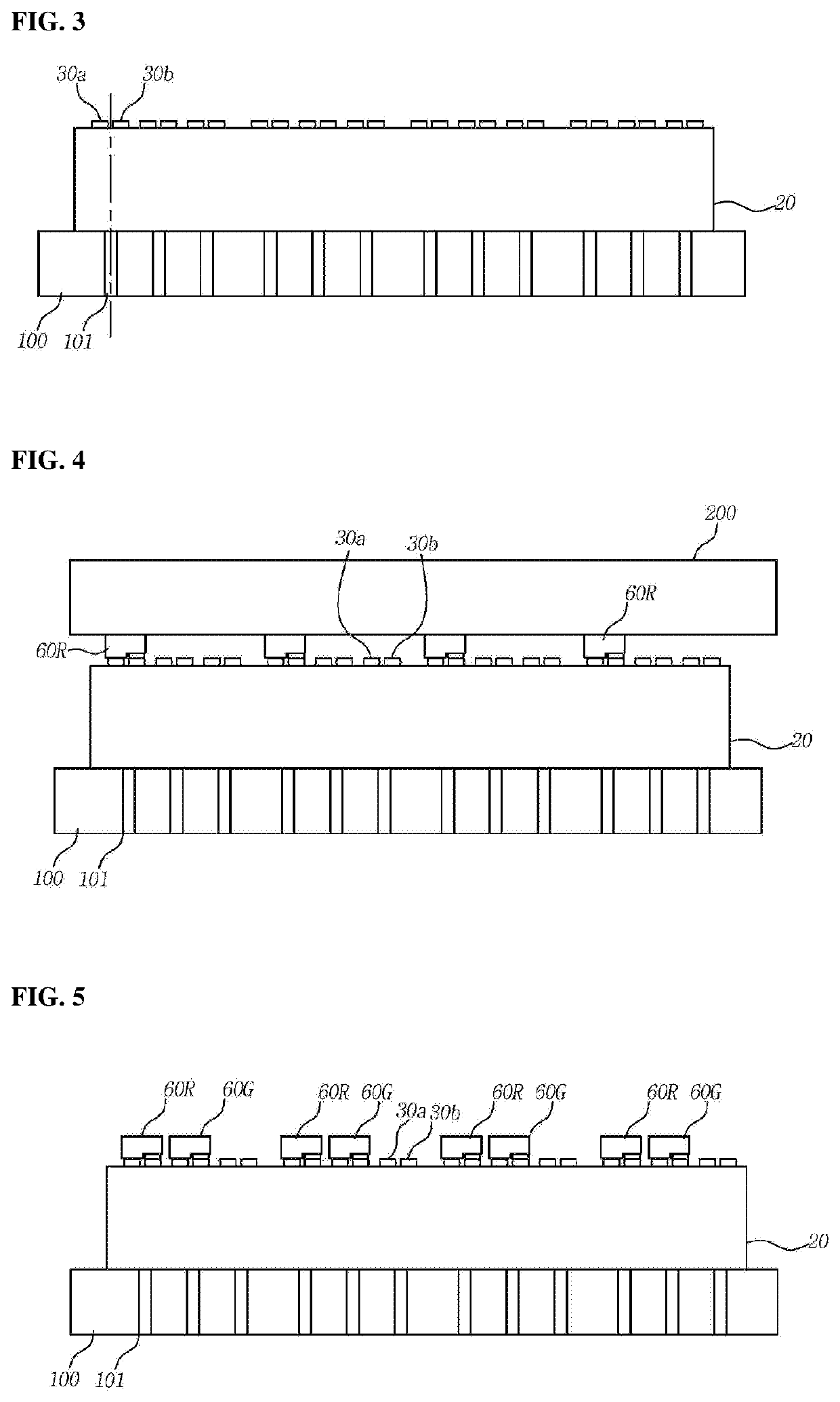
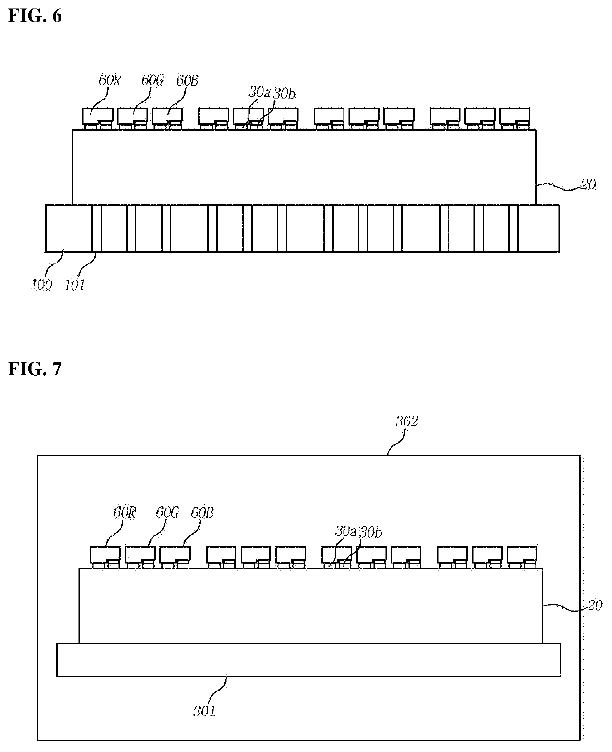
[0038]FIG. 2 illustrates the step of planarizing a circuit board in a method according to one embodiment of the present invention, FIG. 3 illustrates the step of forming solder bumps on the upper surface of the circuit board, FIGS. 4 to 7 illustrate the step of mounting micro-LED chips on the circuit board, and FIGS. 8 and 9 illustrate the step of attaching driver ICs to the lower surface of the circuit board.

[0039]Referring to FIG. 2, a circuit board 20 including an upper surface and a lower surface is prepared. The circuit board 20 may be a printed circuit board (PCB), a flexible circuit board, such as a flexible printed circuit board (FPCB), or a TFT board. A vacuum chuck 100 is prepared to planarize ...


PUM


Abstract

Disclosed is a method for fabricating a micro-LED module. The method includes: preparing a circuit board; forming solder bumps on one surface of the circuit board; arranging micro-LED chips on the one surface of the circuit board such that the micro-LED chips are in contact with the solder bumps; heating the solder bumps to bond the micro-LED chips to the one surface of the circuit board through the solder bumps; arranging driver ICs on the other surface of the circuit board such that the driver ICs are in contact with solders on the other surface of the circuit board in a state in which the micro-LED chips are bonded to the circuit board; and heating the solders to bond the driver ICs to the other surface of the circuit board through the solders. The micro-LED chips are arranged on the one surface of the circuit board after the flatness of the circuit board is enhanced.

Description

BACKGROUND OF THE INVENTION1. Field of the Invention[0001]The present invention relates to a micro-LED module, and more specifically to a method for fabricating a micro-LED module while preventing micro-LED chips from being mounted in incorrect positions on a circuit board attached with driver ICs by poor flatness of the circuit board, and a micro-LED module fabricated by the method.2. Description of the Related Art[0002]A micro-LED display (MLD) typically includes one or more micro-LED modules including a plurality of micro-LED chips. In a broad sense, the term “micro-LED chip” is defined as an LED chip having at least one side whose length is several hundreds of micrometers or less. In a narrow sense, the term “micro-LED chip” is defined as an LED chip having at least one side whose length is a hundred micrometers or less. Particularly, LED chips having at least one side whose length exceeds a hundred micrometers are also called “mini-LED chips”. Herein, LED chips whose sides are ...

Claims


Application Information

Patent Timeline
Patent Type & Authority Applications(United States)
IPC IPC(8): F21V23/00H01L23/492H01L33/18H01L33/48
CPCF21V23/004H01L23/492H01L33/18H01L33/483F21V23/002H01L24/75H01L24/81H01L24/83H01L24/95H01L25/0753H01L25/50H01L33/0095H01L33/62H01L2224/291H01L2224/75303H01L2224/75305H01L2224/75744H01L2224/7598H01L2224/95136H05K3/3431H05K2201/10106H05K2203/082H05K2203/1572Y02P70/50H01L2924/014H01L2924/00014H01L21/6838H01L27/156H01L33/005H01L33/486
Inventor SEO, JUOK
Owner LUMENS
Why Eureka
Try Eureka