
Imprint device and method for manufacturing article

a technology of printing device and printing method, which is applied in the direction of instruments, photomechanical devices, optics, etc., can solve the problems of flatness of substrate and pattern defects, and achieve the effect of reducing pattern defects

Active Publication Date: 2021-12-28
CANON KK
View PDF3 Cites 0 Cited by
  • Summary
  • Abstract
  • Description
  • Claims
  • Application Information

AI Technical Summary

Benefits of technology

The present invention provides an imprint device that can prevent pattern defects caused by unevenness of the substrate.

Problems solved by technology

However, when the pressure sensor is provided at a position facing the mold on the substrate stage, that is, at a position in which the substrate is held, the flatness of the substrate deteriorates and pattern defects can occur.

Method used


Image

  • Imprint device and method for manufacturing article
  • Imprint device and method for manufacturing article
  • Imprint device and method for manufacturing article

Examples


first embodiment

[0016]An aspect for carrying out the present invention will be described below with reference to the drawings and the like.

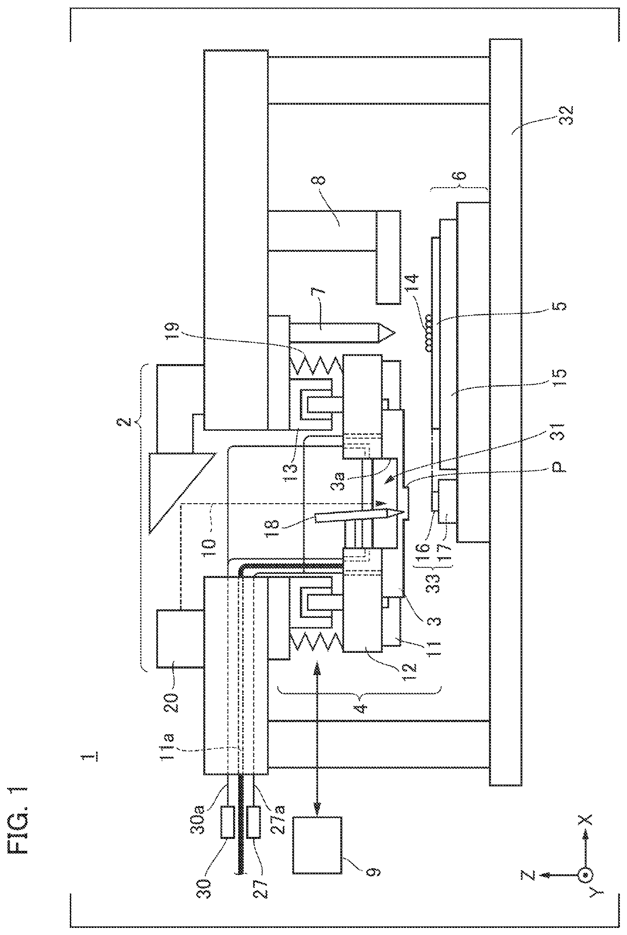
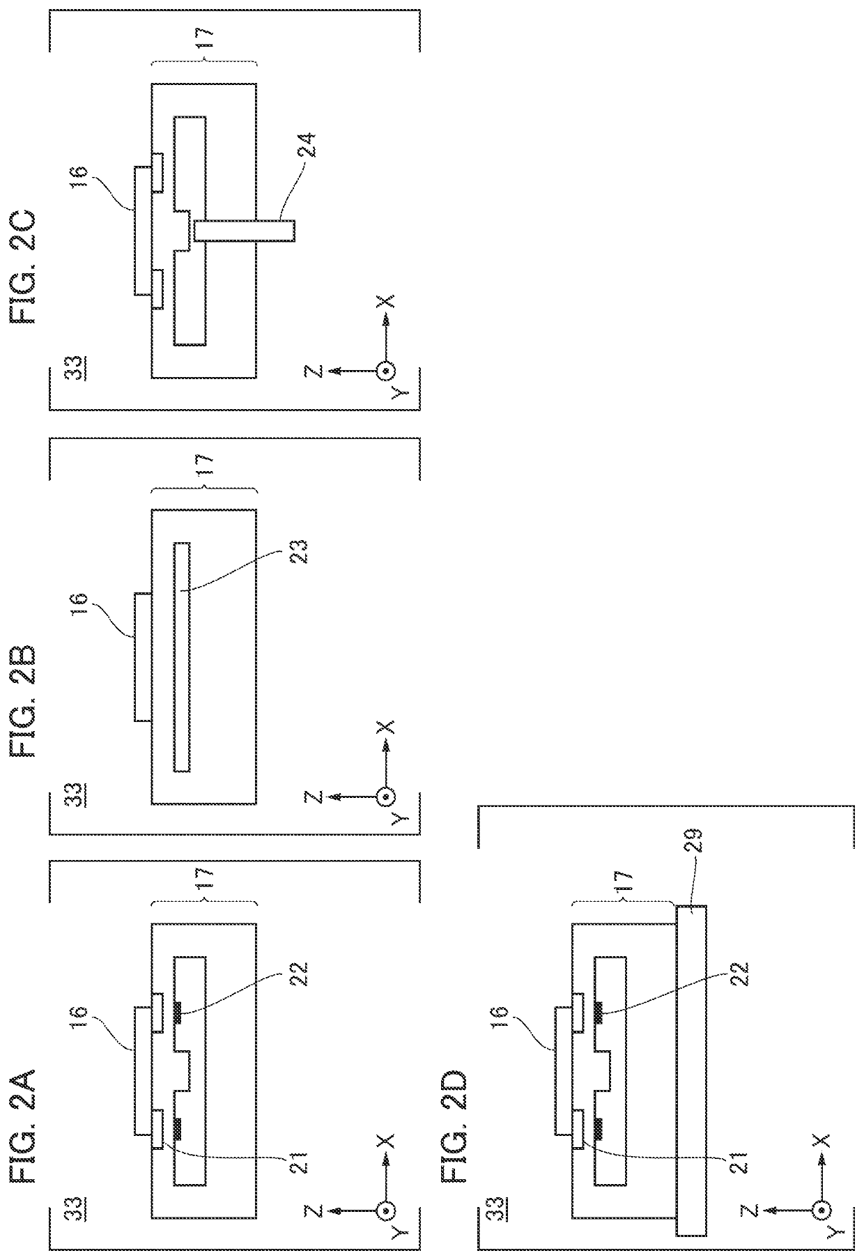
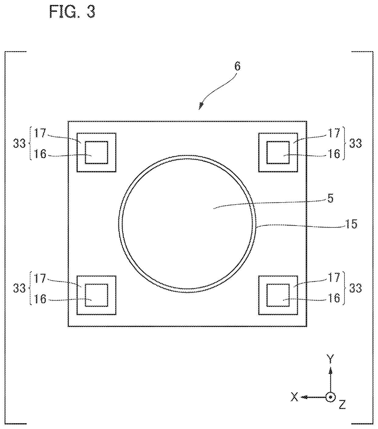
[0017]A configuration of an imprint device according to an embodiment of the present invention will be described first. FIG. 1 is a schematic diagram illustrating a configuration of the imprint device according to a first embodiment. An imprint device 1 in this embodiment is a processing device for imprinting a concave and convex pattern of a mold onto a substrate which is to be processed in a semiconductor device manufacturing process, and is a device to which a light curing method is applied among imprint techniques. The imprint device 1 performs an imprint process of imprinting a pattern formed of an imprint material onto the substrate using the mold. The imprint process is a process of bringing the imprint material on the substrate into contact with the mold (imprinting), curing the imprint material in a contact state, and leaving a pattern formed of the imp...

second embodiment

[0044]An imprint device according to a second embodiment of the present invention will be described below. The matters which are not mentioned in the second embodiment are the same as those in the first embodiment. In the second embodiment, the pressurization using a mold deforming part 30 in a concave portion 3a provided in a mold 3 is also controlled on the basis of the measurement result of a measuring unit 33.

[0045]FIGS. 4A and 4B are diagrams illustrating the measuring unit 33 and the periphery thereof according to a second embodiment. It should be noted that the pressure in the concave portion 3a is measured by the pressure sensor (not shown). First, as illustrated in FIG. 4A, a pattern portion P of the mold 3 is brought into contact with a contact part 16 in a state in which no pressure is applied by the mold deforming part 30 and positional information Z1 of an actuator 13 is acquired when a contact force is measured by the measuring instrument 17. Then, after the mold 3 is ...

third embodiment

[0046]An imprint device according to a third embodiment of the present invention will be described below. The matters which are not mentioned in the third embodiment are the same as those in the first embodiment. In the third embodiment, a displacement sensor 25 is used as a measuring instrument 17 and a contact force is acquired in addition to the rigidity of a mold 3.

[0047]FIG. 5 is a diagram illustrating a measuring unit 33 and the periphery thereof according to the third embodiment. As illustrated in (a) of FIG. 5, in this embodiment, the displacement sensor 25 is used as the measuring instrument 17. The displacement sensor 25 is fixed so that a surface of a contact part 16 facing a mold holding part 12 is used as a reference position and a certain range thereof can be measured in the Z direction. The displacement sensor 25 measures a surface position of a pattern portion P of the mold 3 at the time of contact driving of the mold 3 (at the time of performing driving in the −Z di...


PUM

PropertyMeasurementUnit
heightaaaaaaaaaa
wavelength rangeaaaaaaaaaa

Abstract

In order to provide an imprint device capable of reducing pattern defects, the imprint device which brings a mold into contact with an imprint material on a substrate and transfers a shape of a surface of the mold onto the substrate includes: a mold holding part which holds the mold; a substrate holding part which holds the substrate; and a measuring unit which measures a contact force generated when a part of the mold or the mold holding part is brought into contact with a predetermined contact part, wherein the contact part is installed at a position in a predetermined plane different from a position in the predetermined plane of the substrate held by the substrate holding part and is installed at a height position corresponding to a height of a surface of the substrate held by the substrate holding part.

Description

BACKGROUND OF THE INVENTIONField of the Invention[0001]The present invention relates to an imprint device and a method for manufacturing an article.Description of the Related Art[0002]There is a demand for reducing a size of a semiconductor device, an MEMS, or the like, and therefore a microfabrication technique for imprinting an uncured imprint material on a substrate using a mold having a pattern portion and forming a pattern of the imprint material on the substrate has attracted more attention than conventional photolithography techniques. This technique is so-called an imprint technique and it is possible to form a fine structure on the order of several nanometers on a substrate. Examples of the imprint technique include a light curing method, in which an uncured imprint material is first supplied on a substrate, then the imprint material on the substrate is brought into contact with a pattern portion of a mold, and so that a pattern of an imprint material corresponding to a fin...

Claims


Application Information

Patent Timeline
Patent Type & Authority Patents(United States)
IPC IPC(8): G03F7/00H01L21/027B29C59/00B29C59/02G03F7/20
CPCG03F7/0002B29C59/00H01L21/0271B29C59/02B29C59/022B29C59/026B29C2059/023G03F7/70483G03F7/70491G03F7/70766G03F7/70775G03F7/70825H01L21/027H01L21/67063G03F7/7035G03F7/706851G03F7/70866G03F7/70516G03F7/7085G03F7/7095
Inventor TORII, HIROTOSHI
Owner CANON KK
Learn More