Panel with multiple conductive patterns
a technology of conductive patterns and panels, applied in the field of panels, can solve the problems of complex manufacturing procedures and further raise the difficulty, and achieve the effect of simplifying the manufacturing steps of the touch lin
- Summary
- Abstract
- Description
- Claims
- Application Information
AI Technical Summary
Benefits of technology
Problems solved by technology
Method used
Image

Examples
Embodiment Construction
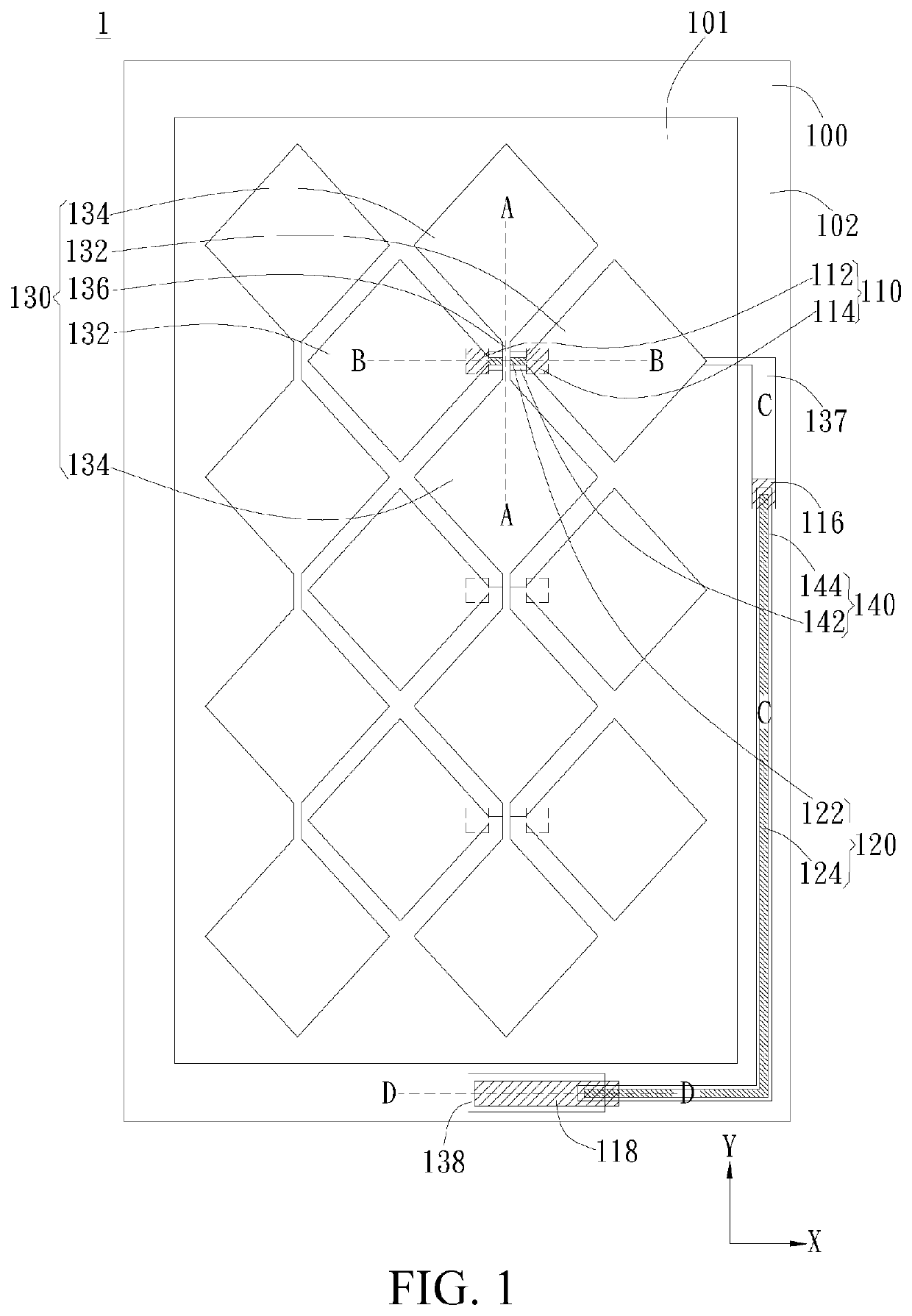
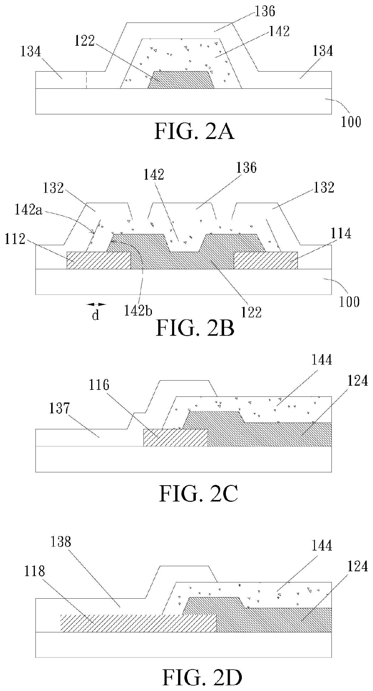
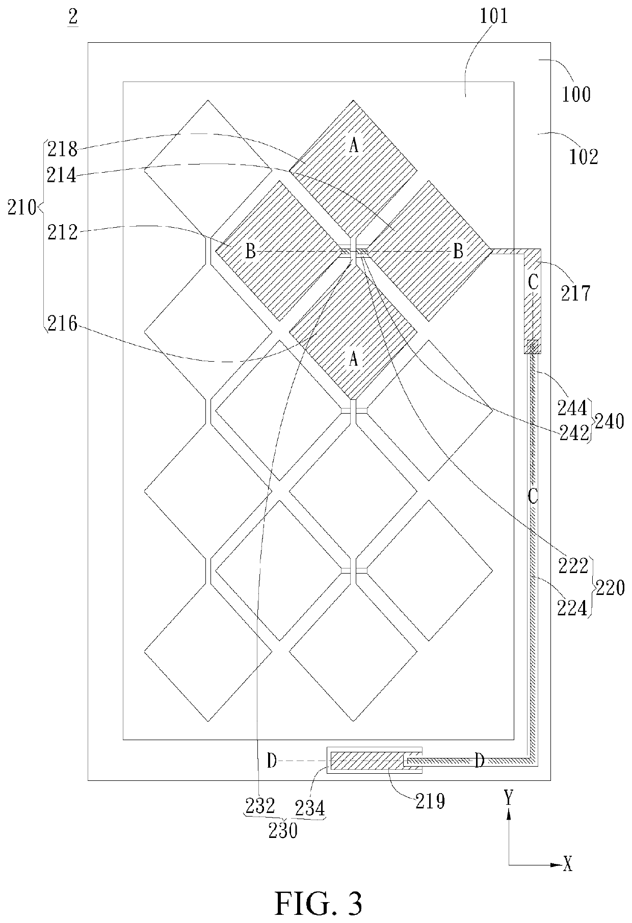
[0029]The present invention provides a panel and a manufacturing method thereof, in particular, a panel whose manufacturing steps are effectively simplified and material costs are effectively saved and a manufacturing method thereof; according to one embodiment of the present invention, a mask pattern used in a patterning step is used as an insulation layer of a bridging portion of adjacent conductive electrodes and / or a light shield layer of a metal line, so as to effectively simplify manufacturing steps, save material costs, and improve light reflection of the metal line. Specifically, the panel of the present invention may be any panel that needs an insulation layer to isolate lines, for example, a touch panel, or a touch display panel that integrates touch and display functions, but the present invention is not limited thereto. Subsequently, details of a panel and a manufacturing method thereof of embodiments of the present invention are described in detail with reference to the...
PUM
 Abstract
Description
Claims
Application Information
 - Generate Ideas
- Intellectual Property
- Life Sciences
- Materials
- Tech Scout
- Unparalleled Data Quality
- Higher Quality Content
- 60% Fewer Hallucinations
Browse by: Latest US Patents, China's latest patents, Technical Efficacy Thesaurus, Application Domain, Technology Topic, Popular Technical Reports.
© 2025 PatSnap. All rights reserved.Legal|Privacy policy|Modern Slavery Act Transparency Statement|Sitemap|About US| Contact US: help@patsnap.com