Semiconductor chip and method of manufacturing semiconductor chip

Active Publication Date: 2007-04-19
SHINKO ELECTRIC IND CO LTD
View PDF10 Cites 38 Cited by
  • Summary
  • Abstract
  • Description
  • Claims
  • Application Information

AI Technical Summary

Benefits of technology

[0023] According to at least one embodiment of the present invention, the Au bump is formed on the electrode pad and in the through hole on the side corresponding to the first principal surface after the insulating film forming step, so that an electrical connection can more easily be established between the electrode pad and the through via, compared with the conventional semiconductor chip. This can simplify the manufacturing steps of the semiconductor chip, and can also reduce the manufacturing cost of the semiconductor chip.
[0024

Problems solved by technology

In the semiconductor chip 100 having a conventional structure as described above, however, the conductive metal member 104 and/or the metal layer 108 are provided to electrically connect the electrode pad 103 with the through via 111, giving rise to the problem of cost increases.
Further, the provision of the conductive metal member 104 and the metal laye

Method used


Image

  • Semiconductor chip and method of manufacturing semiconductor chip
  • Semiconductor chip and method of manufacturing semiconductor chip
  • Semiconductor chip and method of manufacturing semiconductor chip

Examples


Embodiment Construction

[0047] In the following, embodiments of the present invention will be described with reference to the accompanying drawings.

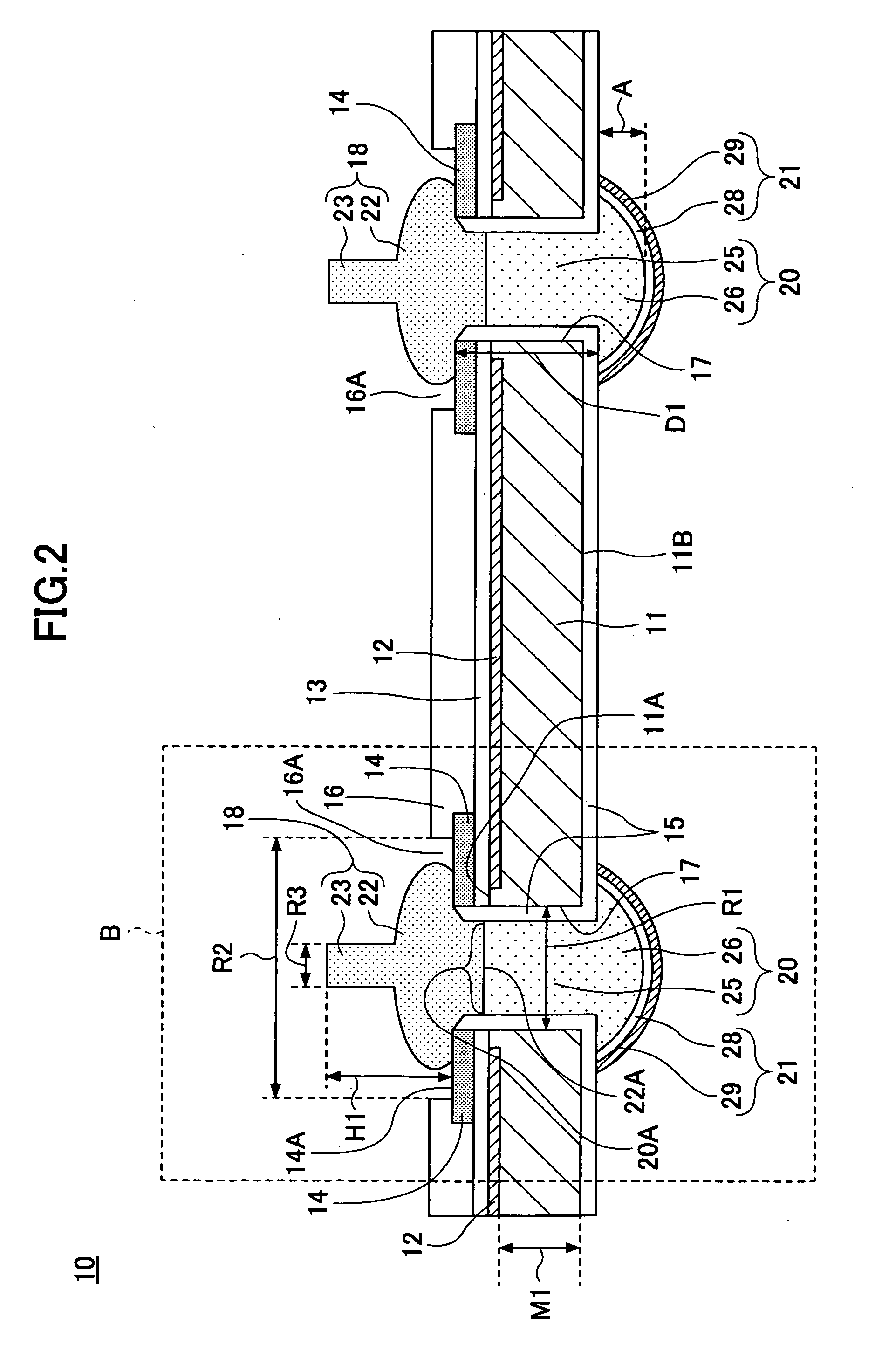
[0048]FIG. 2 is a cross-sectional view of a semiconductor chip according to an embodiment of the present invention. In FIG. 2, “A” represents the elevation of a projection 26 relative to an insulating film 15 that is disposed on a second principal surface 11B of a semiconductor substrate 11, and will hereinafter be referred to as a “projection elevation A”. “D1” represents the depth of a through hole 17, and will hereinafter be referred to as a “depth D1”. “H1” represents the height of an Au bump 18 with reference to an upper surface 14A of an electrode pad 14, and will hereinafter be referred to as a “height H1”.

[0049] As shown in FIG. 2, a semiconductor chip 10 includes a semiconductor substrate 11, a semiconductor-device layer 12, insulating films 13 and 15, electrode pads 14, a protection film 16, Au bumps 18, through vias 20, and dispersion preventive fi...


PUM


Abstract

A semiconductor chip includes a semiconductor substrate having a first principal surface, and having a device layer on the first principal surface in which a semiconductor device is formed, an electrode pad disposed on the first principal surface of the semiconductor substrate and electrically connected to the semiconductor device, a through via formed in a through hole penetrating through the semiconductor substrate and the electrode pad, and an Au bump deposited on the electrode pad and the through via such as to electrically connect between the electrode pad and the through via.

Description

BACKGROUND OF THE INVENTION [0001] 1. Field of the Invention [0002] The present invention generally relates to semiconductor chips and methods of manufacturing semiconductor chips, and particularly relates to a semiconductor chip and a method of manufacturing a semiconductor chip that is provided with a through via penetrating through the semiconductor substrate and electrode pads. [0003] 2. Description of the Related Art [0004] Keeping pace with the recent sophistication and miniaturization of electronic devices, there has been progress in the development of multi-chip packages in which a plurality of semiconductor chips are stacked one over another. Semiconductor chips used in multi-chip packages have a through via that is electrically connected to other semiconductor chips disposed on its top and beneath its bottom. Such through via includes one that is formed to penetrate through the semiconductor substrate and an electrode pad as shown in FIG. 1. [0005]FIG. 1 is a cross-section...

Claims


Application Information

Patent Timeline
IPC IPC(8): H01L23/02H01L21/00
CPCH01L21/568H01L21/6835H01L2924/0002H01L2224/0401H01L2224/05567H01L2924/014H01L2924/01006H01L21/76898H01L23/481H01L24/11H01L24/12H01L24/16H01L24/81H01L25/50H01L2221/68372H01L2224/1134H01L2224/13009H01L2224/13025H01L2224/13144H01L2224/16237H01L2224/81193H01L2224/81203H01L2224/81205H01L2224/81801H01L2225/06513H01L2225/06541H01L2924/01013H01L2924/01029H01L2924/01033H01L2924/01078H01L2924/01079H01L2924/10329H01L2924/00013H01L2924/01005H01L2924/00014H01L2224/13099H01L2224/05552H01L2924/12042H01L2224/05624H01L2224/05576H01L2224/05571H01L2224/16146H01L2224/14181H01L2224/119H01L2224/039H01L24/03H01L24/13H01L24/05H01L2924/00H01L23/48
Inventor SUNOHARA, MASAHIROHIGASHI, MITSUTOSHI
Owner SHINKO ELECTRIC IND CO LTD
Why Eureka
Try Eureka