Semiconductor device and method for manufacturing the same

a semiconductor device and semiconductor technology, applied in semiconductor devices, semiconductor/solid-state device details, variable height tables, etc., can solve the problems of complex etching steps, high cost, and reduced yield rate of semiconductor devices, and achieve the effect of simplifying the whole manufacturing process of semiconductor devices

Inactive Publication Date: 2006-10-31
TAIWAN SEMICON MFG CO LTD
View PDF25 Cites 39 Cited by
  • Summary
  • Abstract
  • Description
  • Claims
  • Application Information

AI Technical Summary

Benefits of technology

[0016]A first object of the present invention is to provide a method for manufacturing a semiconductor device capable of surely exposing projection electrodes by a simple step, and therefore capable of simplifying the whole manufacturing steps of the semiconductor device.
[0017]A second object of the present invention is to provide a method for manufacturing a semiconductor device capable of satisfactorily performing a back side grinding treatment of a semiconductor substrate by preventing the semiconductor substrate from being warped, and thereby capable of favorably manufacturing a thin-type semiconductor device.

Problems solved by technology

Therefore, excessive pursuit of thinning of a semiconductor chip causes the wafer or the semiconductor chip to be broken, so that the yield rate is reduced.
Especially nowadays, since wafers become large-diametered, wafers thinned by the back side grinding treatment are apt to be broken.
At the time of etching, etching conditions must be determined so as to surely expose all of the projection electrodes, and therefore, the etching step is complicated and takes much time.
Furthermore, according to the above-mentioned manufacturing method of the prior art, there is a problem that a wafer is warped because of the differences between the thermal expansion / contraction coefficients of the wafer and the resin layer during the time after forming the resin layer on the wafer and before grinding the back side of the wafer.
Consequently, semiconductor chips each having a uniform thickness cannot be obtained and in addition, sometimes a semiconductor chip cut out of the central region of the wafer may not be thinned to a desired thickness.
Therefore, it is a defect that the whole height (a+b+c) becomes relatively high.
Therefore, the three-dimensional packaging steps are complicated and hard to perform.
Further, in this structure, since the outer leads 75 are pulled outwardly, there is a problem that the area occupied by the whole of the semiconductor device 70 becomes relatively large.

Method used


Image

  • Semiconductor device and method for manufacturing the same
  • Semiconductor device and method for manufacturing the same
  • Semiconductor device and method for manufacturing the same

Examples


second embodiment

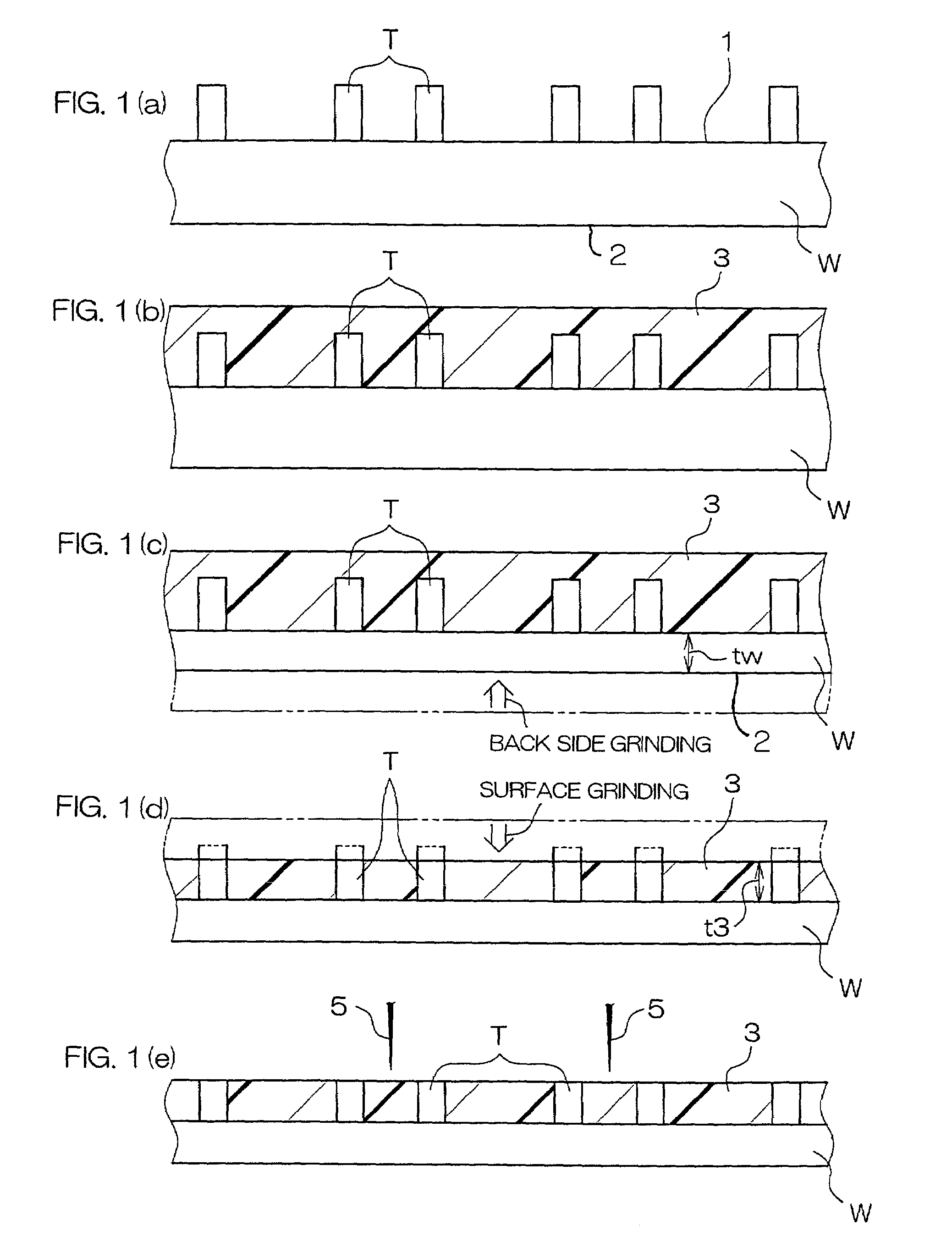
[0088]FIGS. 3(a) to 3(f) are schematically sectional views showing steps in order of a method for manufacturing a semiconductor device according to the present invention. In FIGS. 3(a) to 3 (f), parts corresponding to the parts in FIGS. 1(a) to 1(e) are given the same reference characters with those of the parts in FIGS. 1(a) to 1 (e).

[0089]A semiconductor wafer W (hereinafter referred to simply as wafer W) shown in FIGS. 3(a) to 3(e) has been subjected to a variety of element forming steps, wiring forming steps and the like, and its surface 1 on an active surface layer region side is covered with a protective layer (passivation layer) comprising a nitride layer. A pad (not shown) for external electric connection is exposed from the protective layer.

[0090]As shown in FIG. 3(a), a plurality of projection electrodes T made of, for example, gold (Au) are formed on the pad (electrode forming step). Preferably, these projection electrodes T are formed by, for example, electrolytic platin...

third embodiment

[0102]FIG. 5 is a perspective view showing the structure of a semiconductor device according to the present invention. The semiconductor device 10 has a chip-on-chip structure in which a secondary chip D (the second chip) is bonded face-down onto the surface (active surface) of a primary chip M(the first chip) with the surfaces (active surfaces) of the two chips M,D opposed to each other. Each of the primary chip M and the secondary chip D is formed of, for example, a silicon chip, and active elements such as a transistor, passive elements such as a resistance and a capacitor, wiring or the like are formed on the surface of each chip.

[0103]In this embodiment, each of the primary chip M and the secondary chip D is formed in a rectangular shape when viewed inplan, and the secondary chip D is somewhat smaller than the primary chip M when viewed in plan. A plurality of projection electrodes (cylindrical electrodes in this embodiment) T functioning as external connection electrodes are p...

seventh embodiment

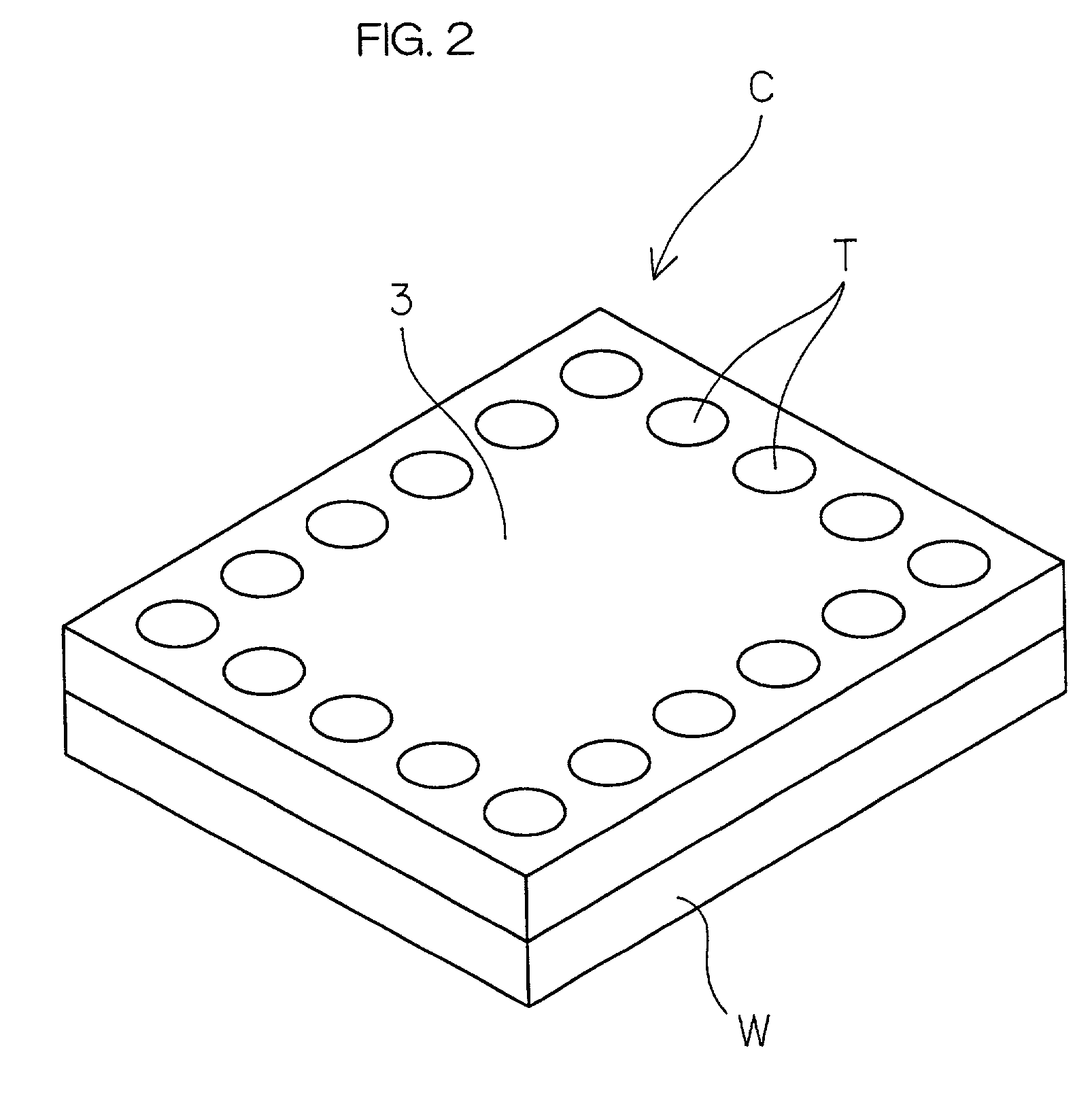
[0119]FIG. 10 is a perspective view showing the structure of a semiconductor device according to the present invention. The semiconductor device 20 has a structure in which a semiconductor chip C is bonded face-down onto the surface of a tape-shaped wiring substrate 21 such as a polyimide substrate or a glass epoxy substrate with the active surface of the semiconductor chip C opposed to the surface of the substrate 21. In this embodiment, the semiconductor chip C is formed in a rectangular shape when viewed in plan. A plurality of projection electrodes (cylindrical electrodes in this embodiment) T protruded from the surface of the substrate 21 and functioning as external connection electrodes are provided in a region surrounding the semiconductor chip C.

[0120]The region, in which the semiconductor chip C or the projection electrodes T are not provided, of the surface of the substrate 21 is resin-sealed with a protective resin (for example, epoxy resin) 25. The protective resin 25 re...


PUM

PropertyMeasurementUnit
heightaaaaaaaaaa
thicknessaaaaaaaaaa
thickness twaaaaaaaaaa

Abstract

A method for manufacturing a semiconductor device having projection electrodes on the surface of a semiconductor substrate. This method include an electrode forming step of forming the projection electrodes on the surface of the semiconductor substrate, a step of forming a protective resin layer on the whole surface of the semiconductor substrate provided with the projection electrodes, a back side grinding step of thinning the semiconductor substrate by polishing or grinding the back side of the semiconductor substrate, and a surface grinding step of exposing the projection electrodes by polishing or grinding the surface side of the semiconductor substrate.

Description

BACKGROUND OF THE INVENTION[0001]1. Field of the Invention[0002]The present invention relates to a method for manufacturing a thin-type semiconductor device. Further, the present invention relates to a semiconductor device having a structure in which a semiconductor chip is bonded onto the surface of a solid device (for example, a wiring substrate or another semiconductor chip), and a method for manufacturing the same.[0003]Further, the present invention relates to a semiconductor device which is advantageous to be three-dimensionally packaged and a method for manufacturing the same.[0004]2. Background Art[0005]A back side grinding step for grinding the back side of a semiconductor wafer (hereinafter referred to simply as wafer) in order to thin a semiconductor chip has been conventionally performed. The back side grinding step has been generally performed by adhering a soft protective film onto the surface of a wafer, then urging the wafer against a grinder through the protective f...

Claims


Application Information

Patent Timeline
Patent Type & Authority Patents(United States)
IPC IPC(8): H01L21/00H01L21/56H01L23/31H01L23/498H01L25/065
CPCH01L21/56H01L21/561H01L23/3107H01L23/49816H01L23/49827H01L24/97H01L25/0655H01L25/0657H01L24/94H01L2224/274H01L2224/97H01L2225/06513H01L2225/0652H01L2225/06541H01L2225/06572H01L2924/0102H01L2924/01029H01L2924/01032H01L2924/01033H01L2924/01074H01L2924/01078H01L2924/01079H01L2924/01082H01L2924/15311H01L2924/15331H01L2924/19041H01L2924/3511H01L2924/01005H01L2924/01006H01L2924/01041H01L2924/01043H01L2224/16225H01L2924/18161H01L2924/10253H01L2924/00H01L2224/16145H01L2224/73209H01L2224/94H01L2224/81H01L2224/82H01L2924/12042H01L2924/181H01L2924/00012H01L21/304
Inventor SHIBATA, KAZUTAKA
Owner TAIWAN SEMICON MFG CO LTD
Why Eureka
Try Eureka