Organic EL element and method of manufacturing the same, organic EL display device using the element, organic EL material, and surface emission device and liquid crystal display device using the material

a technology of organic el and organic el, which is applied in the direction of organic semiconductor devices, discharge tubes/lamp details, natural mineral layered products, etc., can solve the problems of reducing the luminous efficiency, increasing the cost of products, and complicated manufacturing steps, so as to reduce power consumption and increase the utilization factor of light

Inactive Publication Date: 2006-09-14
FUJITSU LTD
View PDF15 Cites 42 Cited by
  • Summary
  • Abstract
  • Description
  • Claims
  • Application Information

AI Technical Summary

Benefits of technology

[0024] Therefore, in view of the above circumstances, it is an object of the present invention to provide an organic EL element and a method of manufacturing the same, that is capable of simplifying its manufacturing steps, lowering the product cost, and avoiding the degradation in the luminescence characteristic and the short-circuit defect of an organic EL layer due to the oxygen and the moisture not to cover a laminated body consisting of an anode, the organic EL layer, and a cathode with an insulating sealing layer, and an organic EL display device employing the organic EL element.
[0025] Also, it is another object of the present invention to provide organic EL material available in practical use, that can be driven by a low voltage, is capable of achieving the reduction in the power consumption, and achieving the cost down and the reduction in size, and a plane emission device and a display device employing the material.

Problems solved by technology

By the way, if the organic EL element is used for a long time, the luminous efficiency is lowered due to the influence of the oxygen and the moisture and also the defect called the dark spot is caused.
As a result, the manufacturing steps become complicated and also the rise of the product cost is brought about.
However, this method has the drawback that the large unevenness is formed.
As a result, there is the possibility that, if the thickness of the organic EL layer is reduced, conversely the short-circuit defect is caused.
But it is difficult to apply the lift-off method to the manufacture of the full-color image display device.
Further, since the organic EL layer is formed of the monomer or polymer organic, such organic EL layer has the drawback that it cannot be worked by the fine pattern technology such as the dry etching, etc.
The cold-cathode lamp, that is employed as the back-light device in the prior art, has the low luminous efficiency and also occupies about 30% of the overall cost of the liquid crystal display device, which is a factor of the cost up.
However, the actual circumstances are that the organic EL material that is available in practical use has not been developed yet.

Method used


Image

  • Organic EL element and method of manufacturing the same, organic EL display device using the element, organic EL material, and surface emission device and liquid crystal display device using the material
  • Organic EL element and method of manufacturing the same, organic EL display device using the element, organic EL material, and surface emission device and liquid crystal display device using the material
  • Organic EL element and method of manufacturing the same, organic EL display device using the element, organic EL material, and surface emission device and liquid crystal display device using the material

Examples


first embodiment

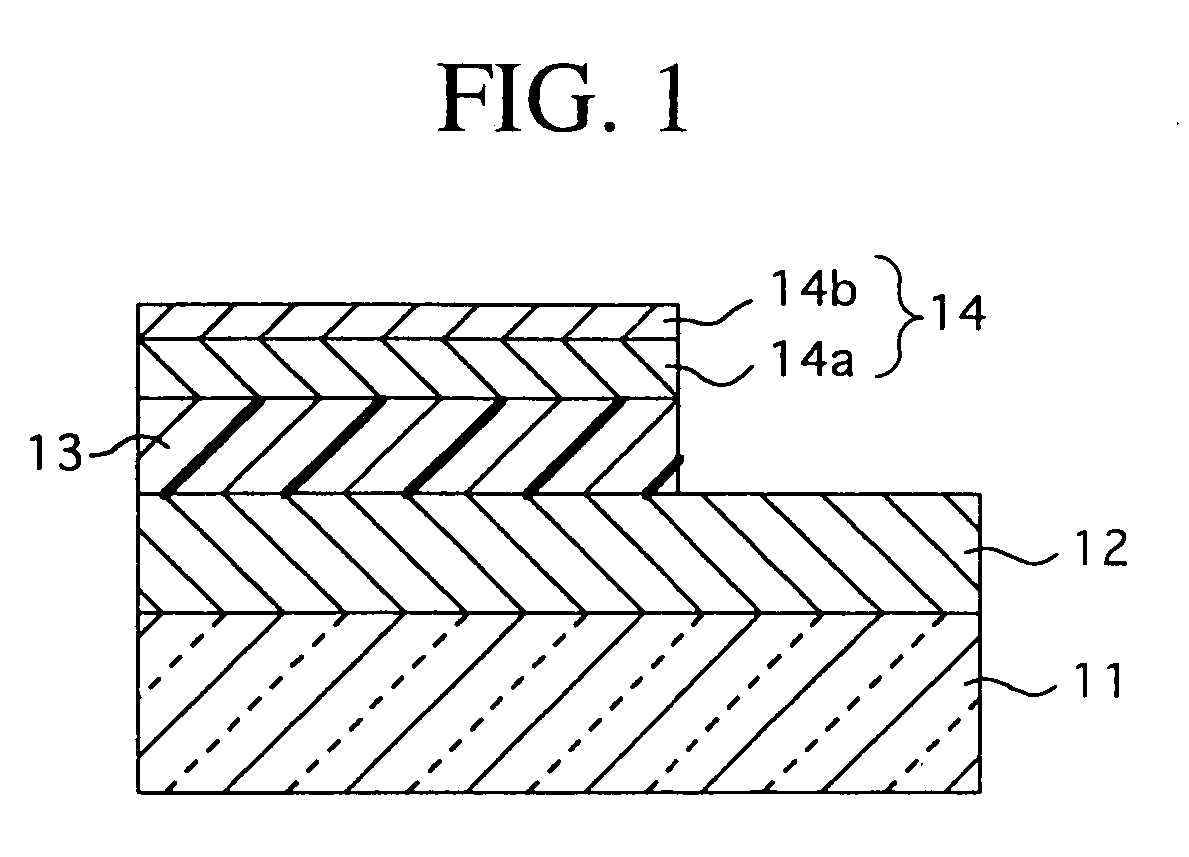
[0097]FIG. 1 is a sectional view showing an organic EL element according to a first embodiment of the present invention.

[0098] An ITO film of about 200 nm thickness is formed as an anode 12 on a glass substrate 11. Also, a poly[3-(4-alkylphenyl)thiophene] film of about 150 nm thickness is formed as an organic EL layer (a luminous layer) 13 in the predetermined area on the anode 12.

[0099] In addition, a laminated film having the double-layered structure consisting of a first conductive film 14a made of the conductor containing Mg and a second conductive film 14b made of the conductor containing Ru is formed as a cathode 14 on the organic EL layer 13. In this example, a thickness of the first conductive film 14a is about 100 nm, and a thickness of the second conductive film 14b is about 50 nm.

[0100] The anode 12 is not limited to ITO, and any conductor having the large work function may be employed. In this case, if the light is irradiated to the substrate 11 side, the anode 12 mus...

second embodiment

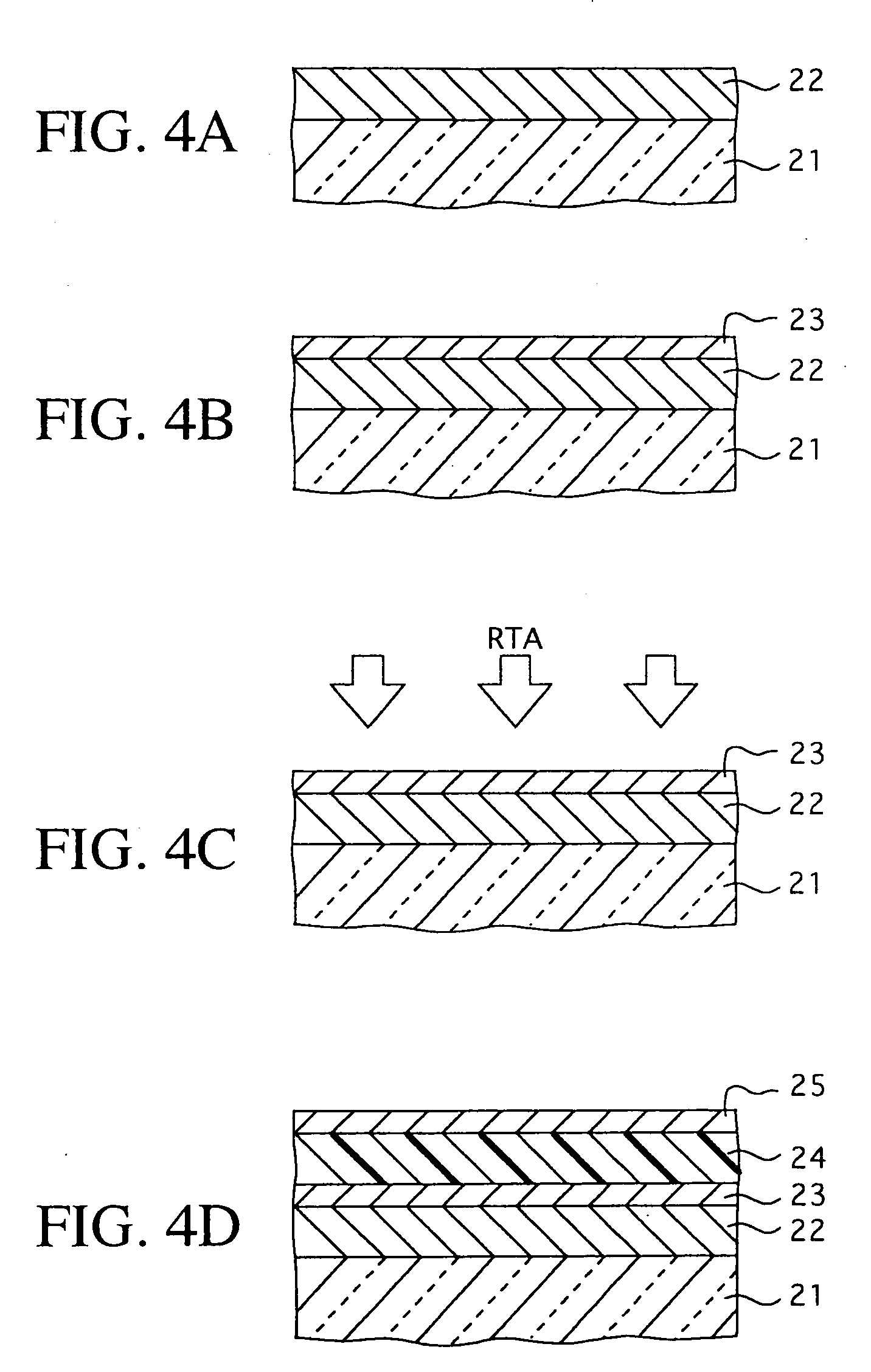
[0118]FIGS. 4A to 4D are sectional views showing a method of manufacturing an organic EL element according to a second embodiment of the present invention.

[0119] The second embodiment shows an example of the organic EL element in which the buffer layer is provided between the anode and the organic EL layer.

[0120] First, as shown in FIG. 4A, the ITO film of 200 nm thickness is formed on an upper side of a glass substrate 21 by the sputter method to construct an anode (lower electrode) 22.

[0121] Then, as shown in FIG. 4B, the Ru (ruthenium) film of 30 nm thickness is formed on the anode 22 by the sputter method to construct a buffer layer 23. Then, as shown in FIG. 4C, the short-time annealing (RTA) is carried out at the temperature of 700° C. for 3 to 5 seconds by using the RTA (Rapid Thermal Annealing) equipment that heats by the lamp.

[0122] The Ru on the surface of the buffer layer 23 is oxidized by this short-time annealing. In this case, since RuO can be generated in a very s...

third embodiment

[0137]FIGS. 5A to 5D are plan views showing manufacturing steps of an organic EL display device according to a third embodiment of the present invention.

[0138] This third embodiment shows an example of a method of manufacturing the full-color organic EL display device.

[0139] First, as shown in FIG. 5A, an ITO film of about 200 nm thickness is formed by sputtering ITO on the overall upper surface of a glass substrate 31. Then, anodes (lower electrodes) 32 are formed by patterning the ITO film into a stripe shape by virtue of the photolithography. In this case, a width of the anode 32 is set to 20 μm, for example.

[0140] Then, an EL emission layer 33 is formed by forming poly[3-(4-alkylphenyl)thiophene] on the overall display area of the glass substrate 31 by virtue of the spin coating method to have a thickness of 1500 Å.

[0141] In the present invention, the material of the EL emission layer 33 is not limited to poly[3-(4-alkylphenyl)thiophene]. But such EL emission layer 33 must b...


PUM

PropertyMeasurementUnit
thicknessaaaaaaaaaa
thicknessaaaaaaaaaa
thicknessaaaaaaaaaa

Abstract

In an organic EL element, an organic EL layer is interposed between anodes and cathodes formed on a substrate. Each of the cathodes is made of a first conductive film that comes into contact with the organic EL layer and a second conductive film that constitutes a laminated structure together with the first conductive film. The first conductive film contains any one of an alkaline metal and an alkaline earth metal. The second conductive film contains any one of at least one type metal selected from a group consisting of Ru (ruthenium), Rh (rhodium), Ir (iridium), Os (osmium) and Re (rhenium) and its oxide.

Description

BACKGROUND OF THE INVENTION [0001] 1. Field of the Invention [0002] The present invention relates to an organic EL (Electroluminescence) element having a structure in which an organic EL layer is put between a pair of electrodes, an organic EL display device employing the element, organic EL material, and a plane emission device and a display device employing the material. [0003] 2. Description of the Prior Art [0004] In recent years, the organic EL element (the organic LED) is well appreciated as the spontaneous emission element. The organic EL element has the advantage that such element can be driven by the low voltage rather than the inorganic EL element and also the advantage that such element can be manufactured without complicated manufacturing processes in contrast to the inorganic LED in the prior art. [0005] Also, in comparison with the liquid crystal display device that is widely used at present as the display of the mobile device, the organic EL element has a quick respon...

Claims


Application Information

Patent Timeline
Patent Type & Authority Applications(United States)
IPC IPC(8): H01L51/54H01L51/52C09K11/06C08G61/00H05B33/14H01L27/32H01L51/30H01L51/50
CPCC07D271/10C07D271/107C08G61/126C09K11/06C09K2211/1425H01L27/32H01L27/3211H01L27/3244H01L27/3281H01L51/0038H01L51/007H01L51/5088H01L51/5221H01L51/5237H01L2251/558H05B33/14Y10S428/917H10K59/35H10K59/00H10K59/17H10K85/114H10K59/12H10K85/6565H10K50/17H10K50/826H10K50/844H10K2102/351
Inventor YOSHIKAWA, KOTA
Owner FUJITSU LTD
Why Eureka
Try Eureka