Semiconductor package and manufacturing method thereof

a technology of semiconductors and packaging, applied in semiconductor devices, semiconductor/solid-state device details, electrical devices, etc., can solve problems such as warpage control, electromagnetic interference becomes critical, and many problems, and achieve good electromagnetic interference shielding and enhanced warpage control

Active Publication Date: 2019-12-12
POWERTECH TECHNOLOGY
View PDF6 Cites 5 Cited by
  • Summary
  • Abstract
  • Description
  • Claims
  • Application Information

AI Technical Summary

Benefits of technology

[0003]Accordingly, the present invention is directed to a package structure and a method of manufacturing thereof, wherein the package structure enhances warpage control and provides good electromagnetic interference (EMI) shielding.

Problems solved by technology

However, with the reduction of product size, many problems such as warpage control and electromagnetic interference becomes critical.

Method used


Image

  • Semiconductor package and manufacturing method thereof
  • Semiconductor package and manufacturing method thereof
  • Semiconductor package and manufacturing method thereof

Examples


Embodiment Construction

[0011]Reference will now be made in detail to the present preferred embodiments of the invention, examples of which are illustrated in the accompanying drawings. Wherever possible, the same reference numbers are used in the drawings and the description to refer to the same or like parts.

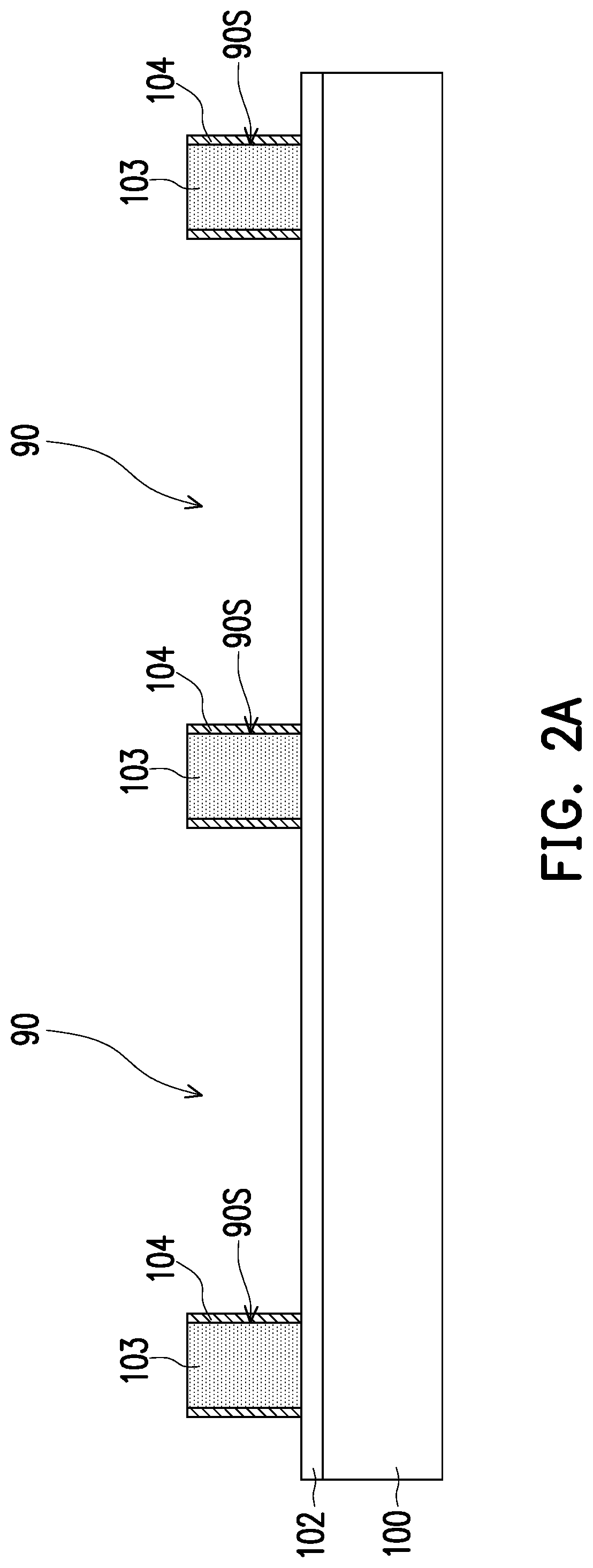
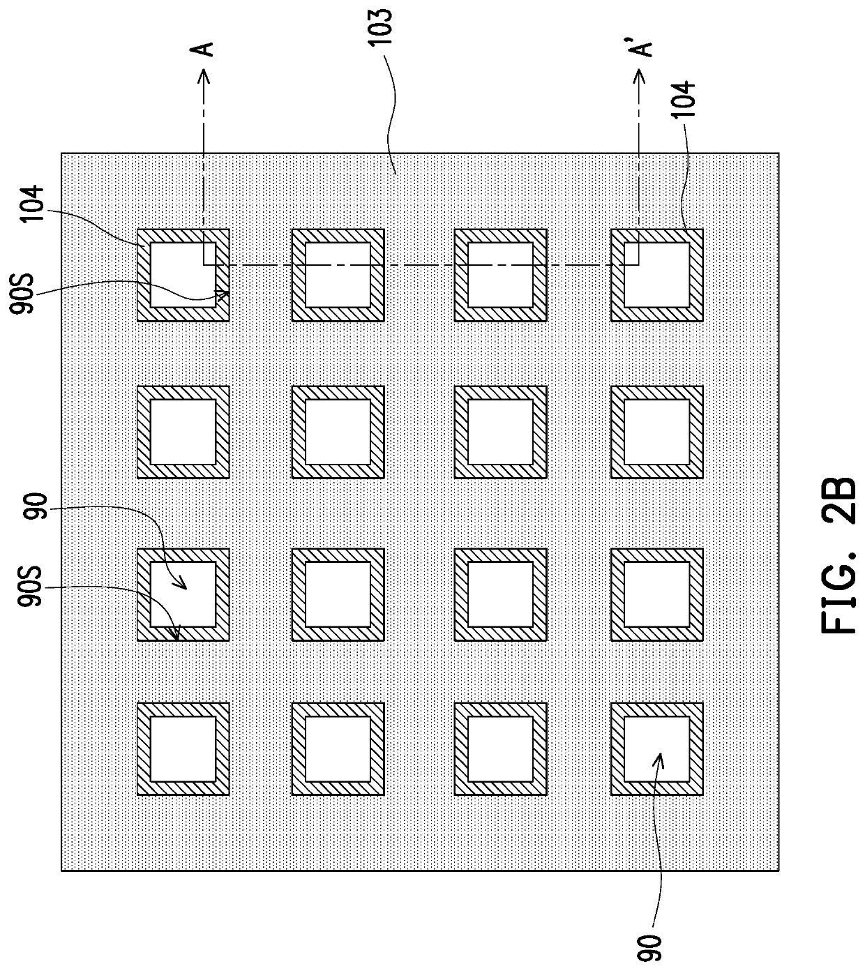
[0012]FIGS. 1 to 10 are schematic cross-sectional views illustrating a manufacturing method of a package structure according to an embodiment of the invention.

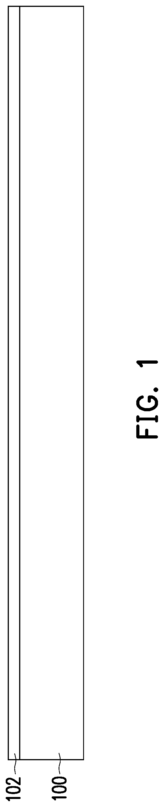
[0013]Referring to FIG. 1, a carrier 100 is provided. In one embodiment, the carrier 100 may be made of silicon, polymer or other suitable materials. In some other embodiments, the carrier 100 may be a glass substrate or a glass supporting board. Other suitable substrate materials may be adapted as the carrier 100 as long as the material is able to withstand the subsequent processes while carrying the package structure formed thereon. As shown in FIG. 1, an adhesive layer 102 is formed on the carrier 100 to enhance the adhesion between the carr...


PUM


Abstract

A package structure including at least one semiconductor chip, an insulating encapsulant, a conductive frame, a supporting frame, a conductive layer and a redistribution layer is provided. The at least one semiconductor chip has an active surface and a backside surface opposite to the active surface. The insulating encapsulant is encapsulating the at least one semiconductor chip. The conductive frame is surrounding the insulating encapsulant. The supporting frame is surrounding the conductive frame. The conductive layer is disposed on the backside surface of the semiconductor chip. The redistribution layer is disposed on and electrically connected to the active surface of the semiconductor chip.

Description

BACKGROUNDTechnical Field[0001]The invention relates to a package structure and a manufacturing method thereof, and more particularly, relates to a package structure that enhances warpage control and provides good electromagnetic interference (EMI) shielding.Description of Related Art[0002]In order for electronic product design to achieve being light, slim, short, and small, semiconductor packaging technology has kept progressing, in attempt to develop products that are smaller in volume, lighter in weight, higher in integration, and more competitive in market. For example, fan-out packages have become increasingly popular due to their compactness. However, with the reduction of product size, many problems such as warpage control and electromagnetic interference becomes critical. Improved reliability provided by integrated fan-out packages having better warpage control and good EMI shielding are the key factors for future packages.SUMMARY[0003]Accordingly, the present invention is d...

Claims


Application Information

Patent Timeline
Patent Type & Authority Applications(United States)
IPC IPC(8): H01L23/00H01L23/552H01L21/48H01L21/56H01L23/31
CPCH01L2224/02379H01L23/552H01L24/09H01L2924/3511H01L24/17H01L23/3107H01L23/562H01L21/56H01L21/4821H01L21/561H01L21/6835H01L23/13H01L23/15H01L23/3128H01L23/49816H01L23/5389H01L24/19H01L24/97H01L2221/68345H01L2224/04105H01L2224/12105H01L2924/3025
Inventor CHANG CHIEN, SHANG-YUHSU, HUNG-HSINLIN, NAN-CHUN
Owner POWERTECH TECHNOLOGY
Why Eureka
Try Eureka