Method for Producing a Component and Component for an Electronic Device

a technology for electronic devices and composite components, applied in semiconductor/solid-state device manufacturing, semiconductor devices, electrical equipment, etc., can solve the problem that the composite components of no material are unnecessarily removed

Active Publication Date: 2019-12-26
OSRAM OLED
View PDF0 Cites 1 Cited by
  • Summary
  • Abstract
  • Description
  • Claims
  • Application Information

AI Technical Summary

Benefits of technology

[0027]According to at least one embodiment of the component, the carrier layer is formed in such a way that it carries the main body. In other words, the carrier layer forms a carrier of the component. In particular, the carrier layer forms the only carrier of the component. The component can be free of a growth substrate. Preferably, the first sublayer is formed as a mechanically stabilizing layer of the carrier layer. As a mechanically stabilizing layer, the first sublayer is form regarding its material and thickness in such a way that it is a self-supporting layer and mechanically stabilizes the component so that the component does not deform or does not deform significantly under its own weight.

Problems solved by technology

This means that no material of the composite of components is unnecessarily removed in the regions of the separating trenches for the purpose of singulating the components.

Method used


Image

  • Method for Producing a Component and Component for an Electronic Device
  • Method for Producing a Component and Component for an Electronic Device
  • Method for Producing a Component and Component for an Electronic Device

Examples


Embodiment Construction

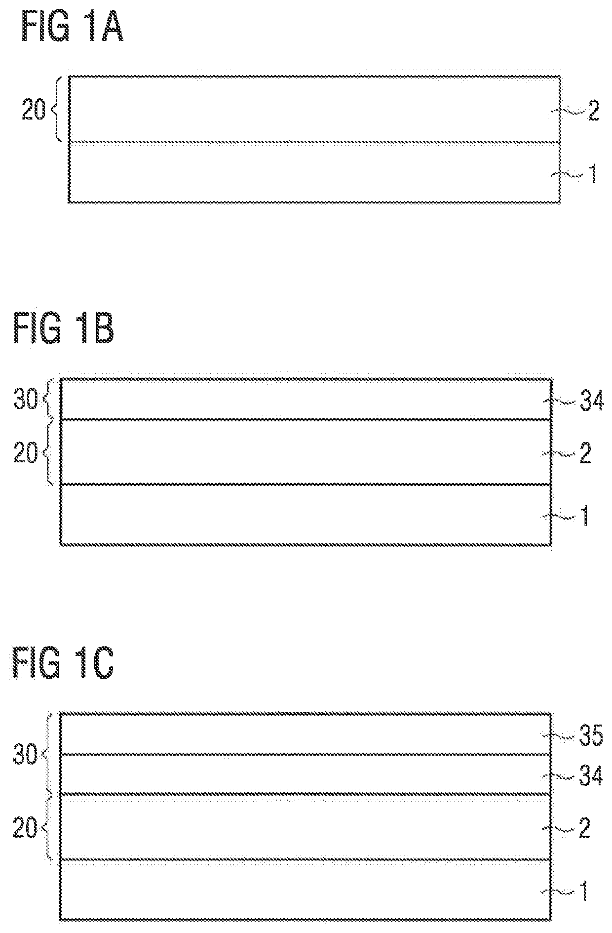
[0034]A substrate 1 is provided in FIG. 1A. On substrate 1, a composite of components of 20 is arranged. In a subsequent method step, the composite of components 20 can be singulated into a plurality of main bodies 2 of the components 10 to be produced. The main body 2 or the composite of components 20 may be a semiconductor body having a plurality of semiconductor layers. In this case, the substrate 1 can be a growth substrate on which the semiconductor layers are grown epitaxially. The growth substrate 1 may be a wafer substrate such as a sapphire substrate, a silicon substrate or a substrate of another semiconductor material. Alternatively, the composite of components 20 is a composite of converter platelets. In this case, the substrate 1 may be different from a growth substrate.

[0035]According to FIG. 1B, an anchoring layer 30 is applied onto the composite of components 20. For this purpose, a first sublayer 34 is first formed for instance over the entire surface of the composit...


PUM


Abstract

A method for producing a component and a component are disclosed. In an embodiment a method includes providing a substrate, applying a composite of components to the substrate, forming an anchoring layer on the composite of components, attaching a carrier to the anchoring layer, wherein the anchoring layer is disposed between the substrate and the carrier and removing the substrate, wherein the composite of components is divided into a plurality of components by forming a plurality of separating trenches, wherein, after removing the substrate, the components continue to be held on the carrier by the anchoring layer, and wherein the anchoring layer comprises at least one predetermined breaking layer having at least one predetermined breaking position, the predetermined breaking position being laterally surrounded by the separating trenches and—in a plan view of the carrier—being covered by one of the components.

Description

[0001]This patent application is a national phase filing under section 371 of PCT / EP2018 / 057013, filed Mar. 20, 2018, which claims the priority of German patent application 102017106730.2, filed Mar. 29, 2017, each of which is incorporated herein by reference in its entirety.TECHNICAL FIELD[0002]A method for producing a component or a plurality of components for electronic devices is specified. Furthermore, a component for an electronic device is specified.BACKGROUND[0003]When transferring components, in particular thin-film semiconductor bodies, preferably, structures are required with which the components can be held stable on a carrier before they can be removed safely and in a targeted manner from the carrier using for instance an adhesive stamp. For this purpose, lateral anchor structures can be formed next to the components. However, these require a comparatively larger surface if the components become smaller, because the lateral anchor structures have to be led out on the si...

Claims


Application Information

Patent Timeline
Patent Type & Authority Applications(United States)
IPC IPC(8): H01L33/00H01L33/62H01L31/02H01L33/50H01L31/0232H01L31/18
CPCH01L31/02322H01L31/186H01L33/50H01L33/62H01L31/02002H01L33/0095H01L21/7806H01L2933/0033H01L2933/0041H01L33/0093
Inventor HÖPPEL, LUTZ
Owner OSRAM OLED
Why Eureka
Try Eureka