Method of manufacturing a field effect transistor device with recessed channel and corner gate device

a field effect transistor and corner gate technology, which is applied in the direction of semiconductor devices, basic electric elements, electrical appliances, etc., can solve the problems of deteriorating the switching characteristics of the transistor, the polysilicon-polysilicon interface disadvantageously deteriorating the electrical resistance of the gate electrode structure, and the planar field effect transistor not scaling well to sub 100 nanometer technologies

Inactive Publication Date: 2007-07-05
POLARIS INNOVATIONS LTD
View PDF16 Cites 28 Cited by
  • Summary
  • Abstract
  • Description
  • Claims
  • Application Information

AI Technical Summary

Benefits of technology

[0019] Preferably, the gate conductor material is polycrystalline silicon (polysilicon). Polysilicon is not reliably removed from vertical surfaces by dry etching when the vertical surfaces are not directly accessible from above. In the prior art, polysilicon residues may therefore remain on the gate oxide in upper sections of the sidewalls of the semiconductor fin. The polysilicon residues or “poly stringers” extend between the gate oxide and the insulator collar along the upper section of the gate groove and the pockets adjacent to the source / drain regions in the semiconductor fin. The poly stringers are electrically connected to the gate electrode and increase the drain-to-gate capacity CDG and the source-to-gate capacity CSG.
[0022] Forming the protection liner comprises the deposition of a conformal protection liner. Then, a sacrificial material is deposited and recessed, such that a residual portion of the sacrificial material forms a sacrificial fill. The sacrificial fill covers the conformal protection liner in the bottom portions of the gate groove and the pockets. In upper portions of the gate groove and the pockets, the protection liner is exposed. The exposed sections of the conformal protection liner are removed. The residual portion of the conformal protection liner forms the protection liner that lines exclusively the bottom sections of the pockets and the gate groove. By use of the sacrificial fill, the upper edge of the protection liner is well controlled.
[0032] By providing the nitride spacer on the inner sidewalls of the opening in the mask stack, a pull back of the oxide mask layer is suppressed, such that in the following a short-circuit between the gate electrode and a source / drain region of the transistor is advantageously avoided.

Problems solved by technology

Planar field effect transistors do not scale down well to sub 100 nanometer technologies, which use a feature size of photolithographic patterns of less than 100 nanometers.
Capacitive coupling between the gate electrode and the source / drain regions deteriorates the switching characteristics of the transistor.
When polycrystalline silicon (polysilicon) is used as the first and the second gate conductor material, a polysilicon-polysilicon interface within the gate groove results from this method, wherein the polysilicon-polysilicon interface disadvantageously deteriorates the electrical resistance of the gate electrode structure.
Experimental results for RCATs fabricated according to the described method show inferior switching characteristics and a wider range for the switching characteristics among a plurality of devices that emerge from the same substrate than expected.
Polysilicon is not reliably removed from vertical surfaces by dry etching when the vertical surfaces are not directly accessible from above.

Method used


Image

  • Method of manufacturing a field effect transistor device with recessed channel and corner gate device
  • Method of manufacturing a field effect transistor device with recessed channel and corner gate device
  • Method of manufacturing a field effect transistor device with recessed channel and corner gate device

Examples


Embodiment Construction

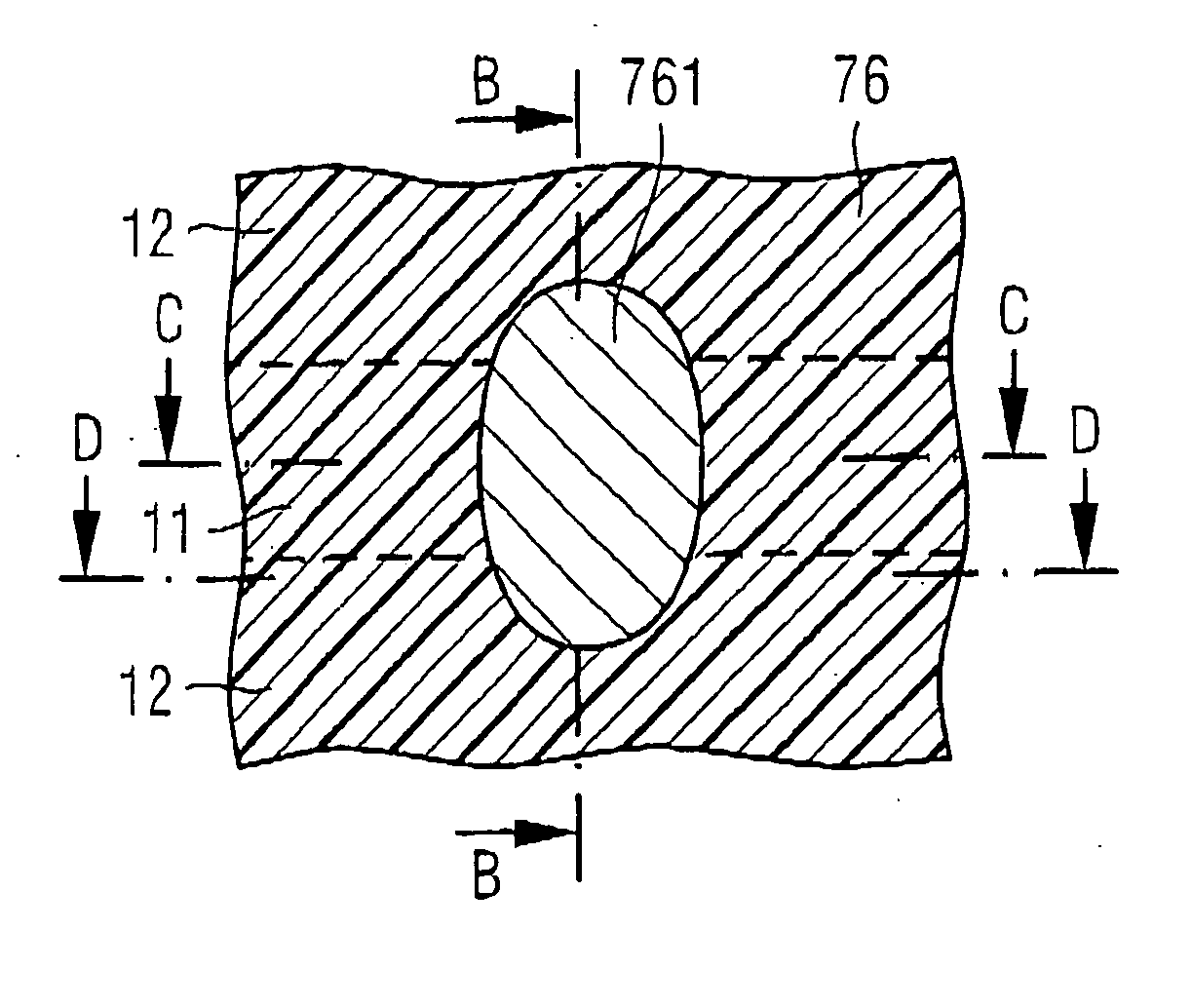
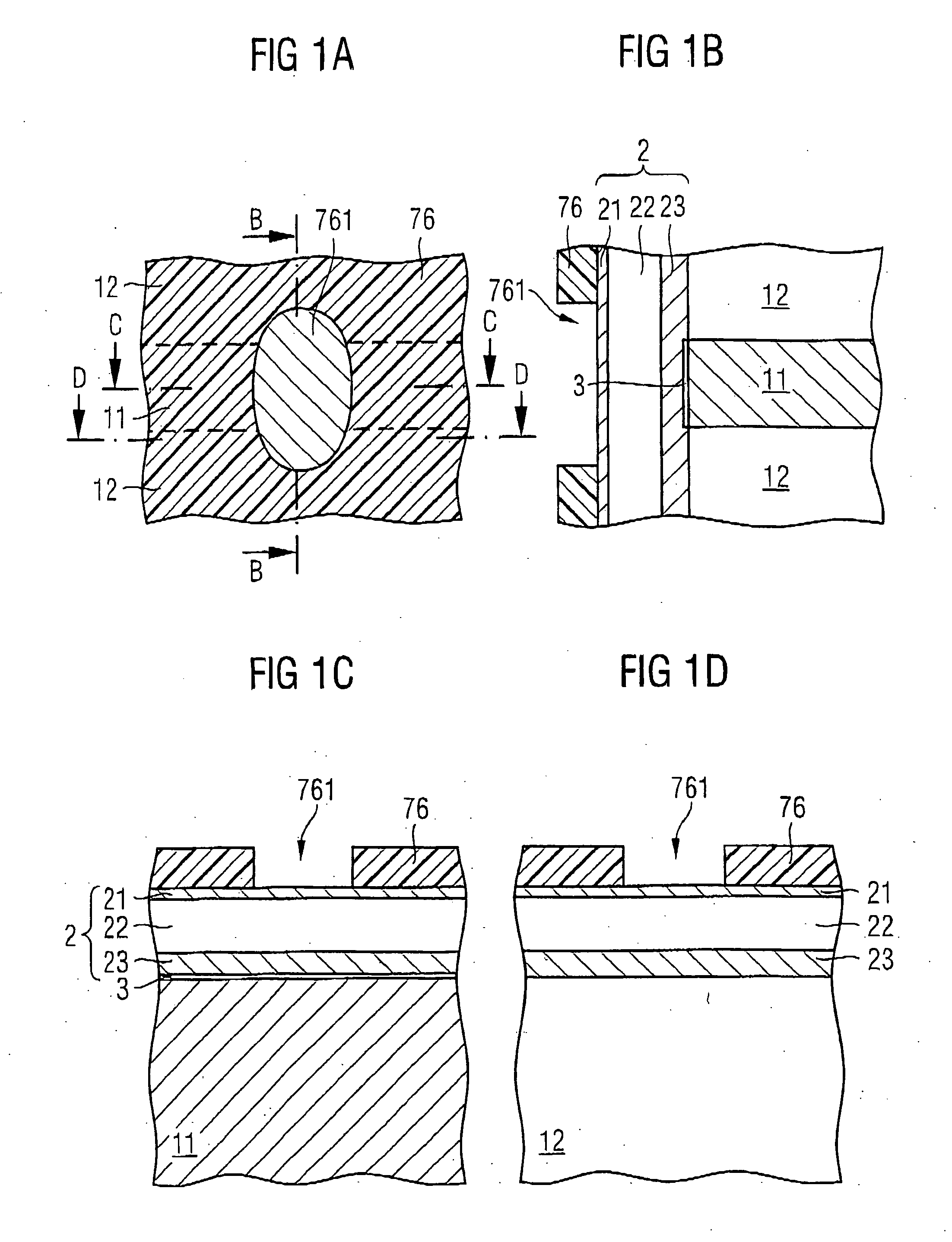
[0041] Referring to FIGS. 1A through 11D, a process of fabricating a recess channel array transistor with corner gate device according to an exemplary embodiment of the invention is shown via plan views and corresponding cross-sectional views, respectively. A semiconductor substrate 1 is provided, which is preferably made of a semiconductor material such as single crystalline silicon. In the semiconductor substrate 1, parallel isolation trenches are formed by photolithographic techniques, wherein a stripe-shaped semiconductor fin 11 with two parallel long sides is formed between the isolation trenches. The isolation trenches are filled with a dielectric material, preferably silicon oxide, such that shallow trench isolations (STI) 12 are formed in the isolation trenches. The shallow trench isolations 12 extend on both long sides of the semiconductor fin 11. A sacrificial oxide 3 covers an upper pattern surface 10 of semiconductor fin 11. The sacrificial oxide 3 may result from a gate...


PUM


Abstract

Fabrication of recessed channel array transistors (RCAT) with a corner gate device includes forming pockets between a semiconductor fin that includes a gate groove and neighboring shallow trench isolations that extend along longs sides of the semiconductor fin. A protection liner covers the semiconductor fin and the trench isolations in a bottom portion of the gate groove and the pockets. An insulator collar is formed in the exposed upper sections of the gate groove and the pockets, wherein a lower edge of the insulator collar corresponds to a lower edge of source / drain regions formed within the semiconductor fin. The protection liner is removed. The bottom portion of the gate groove and the pockets are covered with a gate dielectric and a buried gate conductor layer. The protection liner avoids residuals of polycrystalline silicon between the active area in the semiconductor fin and the insulator collar.

Description

TECHNICAL FIELD [0001] The present invention relates generally to a method of manufacturing a field effect transistor device having a recessed channel and corner gate devices. BACKGROUND OF INVENTION [0002] A semiconductor memory cell typically includes a storage device for storing data and an access device for accessing the data stored in the storage device. [0003] In DRAM memory cells, data is stored by charging or discharging a storage capacitor. In stacked capacitor type memory cells, the capacitors are placed above the access devices. In trench capacitor type memory cells, the storage devices are buried in the substrate in which the access transistors are formed. [0004] Typically the access devices are field-effect transistors (FETs). Active areas of the access transistors are formed in a single crystalline semiconductor substrate such as a silicon wafer. The active areas comprise a first doped region defining a first source / drain region, a second doped region defining a second...

Claims


Application Information

Patent Timeline
Patent Type & Authority Applications(United States)
IPC IPC(8): H01L21/76
CPCH01L27/10876H01L29/4236H01L29/66621H01L29/66553H01L29/66545H10B12/053
Inventor MUEMMLER, KLAUSBAARS, PETERTEGEN, STEFAN
Owner POLARIS INNOVATIONS LTD
Why Eureka
Try Eureka