Electronic Element, Electronic Element Device Using the Same, and Manufacturing Method Thereof

a technology of electronic elements and manufacturing methods, applied in the direction of semiconductor devices, semiconductor/solid-state device details, electrical apparatus, etc., can solve the problems of short-circuiting between electrodes, decomposition and removal of solid-state devices, and complex process, so as to achieve stable and reliable bonding reliability, improve bonding reliability, and ensure the effect of reliability

Active Publication Date: 2009-02-12
MURATA MFG CO LTD
View PDF3 Cites 31 Cited by
  • Summary
  • Abstract
  • Description
  • Claims
  • Application Information

AI Technical Summary

Benefits of technology

[0050]In addition, when the thickness of the metal nanoparticle paste applied onto the first electrode is set to 0.1 μm or more, the thickness of the metal nanoparticle paste sintered body used as the bonding portion can be sufficiently ensured, and when the above thickness is set to 20 μm or less, the dispersing agent and the organic solvent can be sufficiently decomposed and removed even if dispersing agent components of the metal nanoparticle paste are changed, so that it is preferable since the bonding reliability can be stably ensured.
[0051]In addition, when the thickness of the metal nanoparticle paste applied onto the first electrode is set to 15 μm or less, the dispersing agent and the organic solvent can be more reliably decomposed and removed even if dispersing agent components of the metal nanoparticle paste are changed, and it is preferable since the bonding reliability can be further improved.
[0052]In addition, by performing the heating in an atmosphere containing oxygen at a concentration higher than that in the air, the organic components of the dispersing agent and the organic solvent included in the metal nanoparticle paste can be sufficiently decomposed and removed, and hence it is preferable.
[0053]In addition, in a method for manufacturing an electronic element device in which after a bonding material in the form of a paste is applied between an electrode of a first electronic element and an electrode of a second electronic element, the bonding material in the form of a paste is cured so that a bonding portion between the electrode of the first electronic element and the electrode of the second electronic element is formed, when the electrode of said electronic element bonded by the bonding portion is formed by the first to the third steps described above, even if at least one of the first electronic element and the second electronic element has an electrode having a surface composed of at least Al or an Al alloy which is liable to cause a bonding problem due to the presence of an oxide film, an electronic element device having high bonding reliability and electrical conductivity between the electrode of the first electronic element and the electrode of the second electronic element can be obtained.
[0054]In addition, in the method for manufacturing an electronic element device, when the bonding portion between the electrode of the first electronic element and the electrode of the second electronic element is formed in the state in which the electrode of the first electronic element and the electrode of the second electronic element face each other, and even when a fine connection portion must be formed in order to realize high density mounting and to reduce a mounting area by increasing the number of electrodes of the electronic element per unit area, sufficient bonding reliability can be ensured.

Problems solved by technology

However, when the BGA method is used, as the pitches between solder balls are decreased, a so-called bridge is generated during re-flow, and as a result, short-circuiting between electrodes is liable to occur.
In the case as described above, the metal nanoparticle sintered body 208 and the Al oxide film 209 are not sufficiently bonded to each other, and as a result, a problem in that the bonding reliability and the electrical conductivity are degraded may arise.
Hence, the process becomes complicated, and as a result, a problem in that manufacturing cost of the electronic element device is increased may arise.

Method used


Image

  • Electronic Element, Electronic Element Device Using the Same, and Manufacturing Method Thereof
  • Electronic Element, Electronic Element Device Using the Same, and Manufacturing Method Thereof
  • Electronic Element, Electronic Element Device Using the Same, and Manufacturing Method Thereof

Examples


example 1

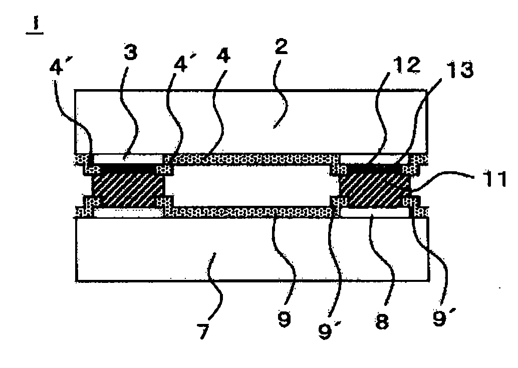
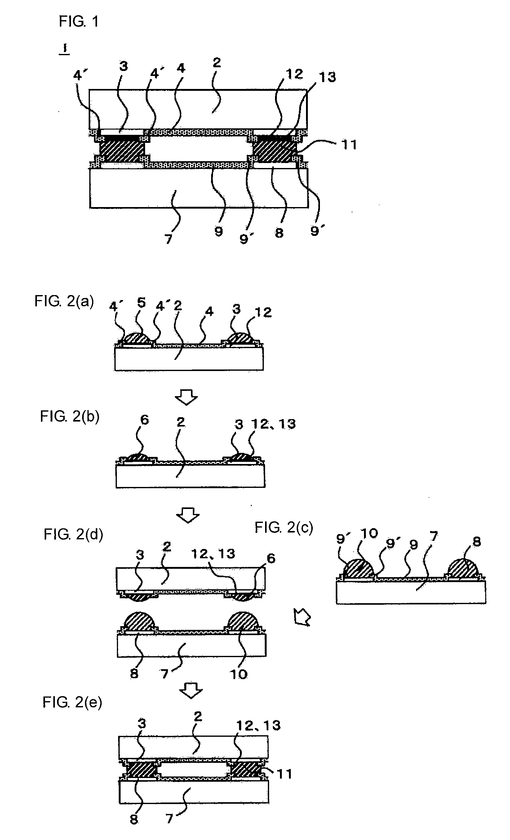
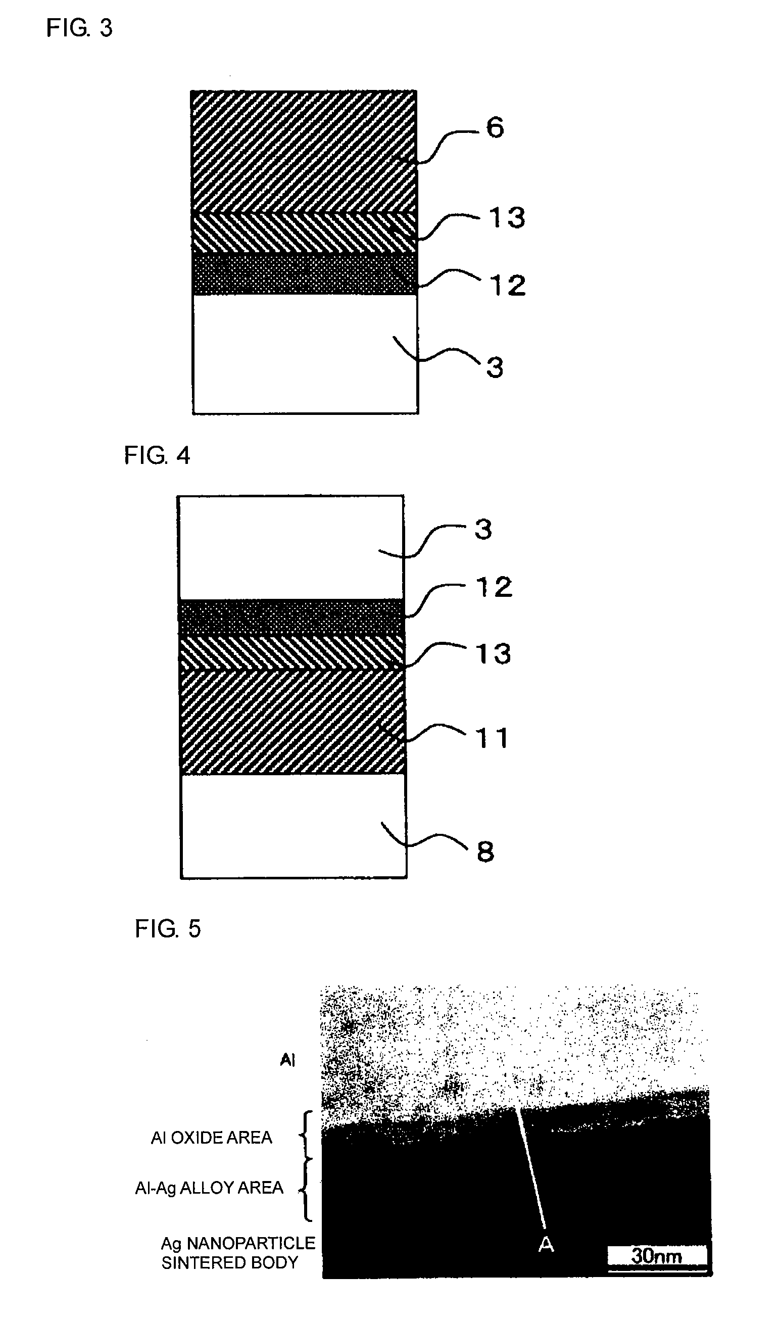
[0114]This example relates to the electronic element device formed by flip chip mounting shown in FIG. 1, and as the electronic element 2 used for the electronic element device 1, a Si-based small semiconductor element was used. The electronic element electrodes 3 disposed on the bottom surface of the electronic element were composed of Al and were formed so as to have a thickness of approximately 0.5 to 2.0 μm. In addition, on the surface of the electronic element electrode 3, the Al oxide film 12 was naturally generated to have a thickness of approximately 5 to 10 nm. On the electronic element 2, the passivation film 4 composed of SiN was disposed. Openings were formed in the passivation film 4 at positions corresponding to the electronic element electrodes 3, and the dam portions 4′ were formed around the openings in order to prevent the spread of a metal nanoparticle paste, which will be described later, by extending parts of the passivation film 4 on the electronic element elec...

example 2

[0137]FIG. 9 shows another example of the present invention. This example relates to an electronic element device having the structure in which a bare chip was mounted on a substrate in a face-up manner, and as an electronic element 14 used for an electronic element device 100, a Si-based semiconductor element was used. Electronic element electrodes 15 and a passivation film 16 were formed on the upper surface of the electronic element 14, and parts of the passivation film 16 were extended on the electronic element electrodes 15 so as to form dam portions 16′.

[0138]In addition, as a substrate 18, a ceramic substrate including a low-temperature firable alumina-based material was used. Substrate electrodes 19 each having a multilayer structure of Cu / Ni / Au were disposed on the upper surface of the substrate 18 and were electrically connected to the electronic element electrodes 15 through Ag nanoparticle sintered bodies 17.

[0139]In this example, the electronic element electrode 15 was ...

example 3

[0141]FIG. 10 shows still another example of the present invention. This example relates to an electronic element device having the structure in which a passive element was mounted on a substrate, and as an electronic element 20 used for an electronic element device 110, a multilayer ceramic capacitor including a BaTiO3-based dielectric material was used. At two ends of the electronic element 20, electrodes 21 each formed by plating Ni / Sn on an underlayer electrode composed of a Cu sintered body were disposed.

[0142]In addition, as a substrate 23, a composite material substrate including a glass epoxy was used. Substrate electrodes 24 each having a single layer structure of Al were disposed on the upper surface of the substrate 23 and were electrically connected to the electronic element electrodes 21 through Ag nanoparticle sintered bodies 22.

[0143]In the case of this example, since the surface of the substrate electrode 24 was covered with the Al oxide film 12, a Ag nanoparticle pa...


PUM

PropertyMeasurementUnit
particle diameteraaaaaaaaaa
thicknessaaaaaaaaaa
thicknessaaaaaaaaaa

Abstract

An electronic element including an electronic element base and electrodes each of which has a first electrode having a surface composed of at least Al or an Al alloy and a second electrode composed of a metal nanoparticle sintered body and bonded to the first electrode. A bonding interface between the first electrode and the second electrode has a multilayer structure including, from the side of the first electrode to the side of the second electrode, (a) a first layer primarily composed of Al, (b) a second layer primarily composed of an Al oxide, (c) a third layer primarily composed of an alloy of Al and a constituent element of metal nanoparticles, and (d) a fourth layer primarily composed of the constituent element of the metal nanoparticles.

Description

CROSS REFERENCE TO RELATED APPLICATIONS[0001]The present application is a continuation of International Application No. PCT / JP2007 / 055290, filed Mar. 15, 2007, which claims priority to Japanese Patent Application No. JP2006-119200, filed Apr. 24, 2006, the entire contents of each of these applications being incorporated herein by reference in their entirety.FIELD OF THE INVENTION[0002]The present invention relates to an electronic element including electrodes each having a surface composed of at least Al or an Al alloy, an electronic element device using the same, and a manufacturing method thereof.BACKGROUND OF THE INVENTION[0003]In recent years, concomitant with reduction in size of electronic apparatuses, higher integration of semiconductor packages has been increasingly required. Even in a mounting technique in which a semiconductor package is mounted on and fixed to a substrate so as to obtain electrical conduction, higher integration and higher density have been required.[0004...

Claims


Application Information

Patent Timeline
Patent Type & Authority Applications(United States)
IPC IPC(8): H01L23/488H01L21/44
CPCH01L24/03H01L24/05H01L24/11H01L24/13H01L24/16H01L24/81H01L2224/0331H01L2224/03505H01L2224/0401H01L2224/05073H01L2224/05124H01L2224/05573H01L2224/05624H01L2224/05639H01L2224/05644H01L2224/05647H01L2224/05794H01L2224/05839H01L2224/1131H01L2224/11505H01L2224/1155H01L2224/13099H01L2224/13139H01L2224/13144H01L2224/13147H01L2224/13294H01L2224/13339H01L2224/245H01L2224/29339H01L2224/29344H01L2224/29347H01L2224/76155H01L2224/81055H01L2224/81097H01L2224/81193H01L2224/8121H01L2224/8123H01L2224/81379H01L2224/81594H01L2224/81639H01L2224/81801H01L2224/8184H01L2224/8284H01L2224/8384H01L2224/94H01L2924/01013H01L2924/01029H01L2924/01033H01L2924/01046H01L2924/01047H01L2924/01058H01L2924/01075H01L2924/01078H01L2924/01079H01L2924/01082H01L2924/014H01L2924/10253H01L2924/10329H01L2924/15165H01L2924/15787H01L2924/19041H01L2224/0558H01L2924/01005H01L2924/01006H01L2924/0105H01L2224/16501Y10S977/779H01L2224/11332H01L2924/00014H01L2924/0543H01L2924/20107H01L2924/01014
Inventor FUNAKI, TATSUYA
Owner MURATA MFG CO LTD
Why Eureka
Try Eureka