Actinic ray-sensitive or radiation-sensitive resin composition, resist film, pattern forming method, and method for manufacturing electronic device
- Summary
- Abstract
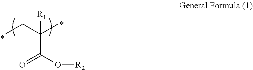
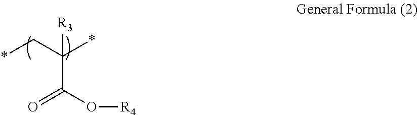
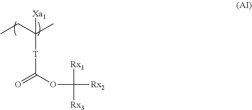
- Description
- Claims
- Application Information
AI Technical Summary
Benefits of technology
Problems solved by technology
Method used
Image

Examples
example 13
Pattern Formation (Example 13)
[0595]Pattern formation was carried out by the same method except that rinsing with pure water and baking at 110° C. for 60 seconds after the drying were not performed in pattern formation (Examples 1 to 12, Examples 14 to 84, and Comparative Examples 1 to 3).
[0596]According to the procedure, a pattern wafer for evaluation, having a substrate and a pattern formed on a surface of the substrate, was obtained.
[0597]
[0598]Performance evaluation of the pattern was carried out using the obtained pattern wafer for evaluation.
[0599](Performance Evaluation 1: Evaluation of Crack Resistance against Vacuum Treatment of Pattern)
[0600]The pattern wafer for evaluation was subjected to a vacuum treatment (evacuation) for 60 seconds in a chamber within a critical dimension-scanning electron microscope (CD-SEM). In addition, the pressure in the chamber was set to 0.002 Pa.
[0601]After the vacuum treatment, the pattern wafer for evaluation was observed with an optical mic...
PUM
| Property | Measurement | Unit |
|---|---|---|
| Temperature | aaaaa | aaaaa |
| Temperature | aaaaa | aaaaa |
| Percent by mass | aaaaa | aaaaa |
Abstract
Description
Claims
Application Information
 - R&D Engineer
- R&D Manager
- IP Professional
- Industry Leading Data Capabilities
- Powerful AI technology
- Patent DNA Extraction
Browse by: Latest US Patents, China's latest patents, Technical Efficacy Thesaurus, Application Domain, Technology Topic.
© 2024 PatSnap. All rights reserved.Legal|Privacy policy|Modern Slavery Act Transparency Statement|Sitemap