Laser annealing method

Inactive Publication Date: 2020-02-06
SAKAI DISPLAY PROD
View PDF0 Cites 0 Cited by
  • Summary
  • Abstract
  • Description
  • Claims
  • Application Information

AI Technical Summary

Benefits of technology

[0004]However, with the conventional SLS method, the growth direction of grain boundaries is limited to th

Problems solved by technology

However, with the conventional SLS method, the growth direction of grain boundaries is limited to the s

Method used


Image

  • Laser annealing method
  • Laser annealing method
  • Laser annealing method

Examples


Example

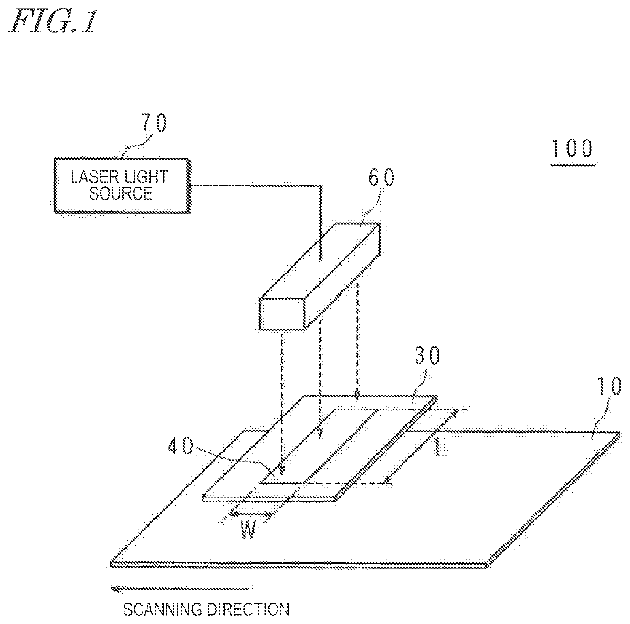
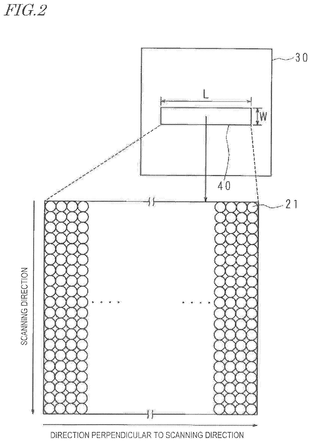
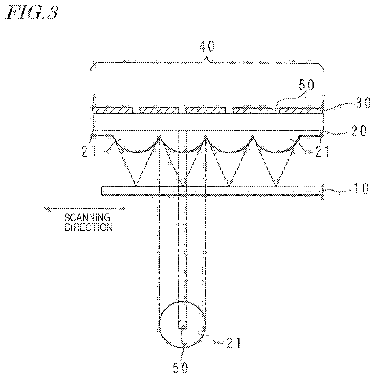
[0027]The present invention will now be described with reference to drawings that show embodiments thereof. FIG. 1 is a schematic view showing an example configuration of a laser annealing apparatus of the present embodiment. A laser annealing apparatus 100 of the present embodiment includes a laser light source 70 that emits laser light, an optical system 60 that includes a group of lenses for shaping the laser light emitted from the laser light source 70 into a parallel beam, a mask (light-blocking plate) 30 that includes a mask portion 40 where openings and microlenses to be described below are arranged in an array, etc. The parallel beam shaped through the optical system 60 selectively irradiates intended locations of a substrate 10 through the openings and the microlenses of the mask portion 40. The substrate 10 is transferred at a constant speed by a driving mechanism (not shown). The laser light source 70 shoots laser light at time intervals such that laser light is shot each...


PUM


Abstract

A laser annealing method includes: step A of providing a substrate having an amorphous semiconductor film formed on a surface thereof; and step BF of selectively irradiating a portion of the amorphous semiconductor film with laser light. Step B includes a step of simultaneously forming, in said portion, a first melted region that is elongated in a first direction and a second direction that is elongated in a second melted region different from the first direction.

Description

BACKGROUND1. Technical Field[0001]The present invention relates to a laser annealing apparatus, a display panel, a laser annealing method and a mask.2. Description of the Related Art[0002]While examples of TFTs (Thin Film Transistors) of liquid crystal displays include amorphous silicon (non-crystalline, a-Si) TFTs and low temperature polysilicon (polycrystalline, p-Si) TFTs, for example, polycrystalline silicon has been often used instead of amorphous silicon in cases where there is a demand for high-speed operations such as with driver circuits, etc.[0003]For crystallization of semiconductor film regions on the substrate, a process is known in the art for growing grain boundaries in the lateral direction parallel to the substrate surface by using a sequential lateral solidification (SLS) method. In the conventional SLS method, intended regions of a silicon film are irradiated with laser light through thin slit openings of a mask so as to completely melt the silicon of the regions,...

Claims


Application Information

Patent Timeline
IPC IPC(8): H01L21/02
CPCH01L21/02686H01L21/02532H01L21/02595H01L21/0268H01L21/02691
Inventor TANAKA, MASAKAZUKOIWA, SHINJIKARATANI, KOUICHISHINOZUKA, AKIHIRONODERA, NOBUTAKEMATSUMOTO, TAKAO
Owner SAKAI DISPLAY PROD
Why Eureka
Try Eureka