Aperture-coupled microstrip-to-waveguide transitions

a technology of waveguides and transitions, applied in waveguides, electrically short antennas, antennas, etc., can solve the problems of waveguide-to-coax adapters not mate well with rf boards, waveguide-to-coax adapters have size, weight, power,

Active Publication Date: 2020-02-27
THE BOEING CO
View PDF0 Cites 14 Cited by
  • Summary
  • Abstract
  • Description
  • Claims
  • Application Information

AI Technical Summary

Benefits of technology

[0007]Further disclosed is a method for fabricating the ACMWT utilizing a three-dimensional (“3-D”) additive printing process. The method includes printing a first conductive layer having a top surface and a first width. The first width has a first center and the first conductive layer is a bottom layer configured as a reference ground plane. The method then includes printing a first dielectric layer on the top surface of the first conductive layer, where the first dielectric layer has a top surface, printing a second dielectric layer on the top surface of the first dielectric layer, where the second dielectric layer has a top surface, and printing a second conductive layer on the top surface of the second dielectric layer. The second conductive layer has a top surface and a second width, the second width is less than the first width, and the second conductive layer is an inner conductor. The method then includes printing a third dielectric layer on the top surface of the second conductive layer and on the top surface on the second dielectric layer, where the third dielectric layer has a top surface, and printing a third conductive layer on the top surface of the fourth third dielectric layer. The third conductive layer has a top surface and a third width, the third width is less than the first width, and the third conductive layer is a CE. The method then includes printing a fourth dielectric layer on the top surface of the third conductive layer and on the top surface of the third dielectric layer, where the fourth dielectric layer has a top surface, and printing a fourth conductive layer on the top surface of the fourth dielectric layer to produce a PAE with an antenna slot. The fourth conductive layer has a fourth width, the fourth width is less than the first width, and the fourth conductive layer includes the antenna slot within the fourth conductive layer that exposes the top surface of the fourth dielectric layer through the fourth conductive layer. The method then includes attaching the waveguide wall to the fourth dielectric layer.

Problems solved by technology

At present, waveguides are used in many RF applications for low-loss signal propagation; however, they are generally not directly compatible with surface-mount device (“SMD”) RF electronics.
Unfortunately, existing waveguide-to-coax adapters do not mate well with RF boards because they are typically bulky devices that include waveguide tubing, flanges and a combination of a coaxial probe assembly with coaxial adapter and connection hardware to connect the coaxial adapter to the RF board.
As such, at present, known waveguide-to-coax adapters have size, weight, and power (“SWaP”) characteristics and costs that are not compatible with low-cost and conformal RF applications.

Method used


Image

  • Aperture-coupled microstrip-to-waveguide transitions
  • Aperture-coupled microstrip-to-waveguide transitions
  • Aperture-coupled microstrip-to-waveguide transitions

Examples


Embodiment Construction

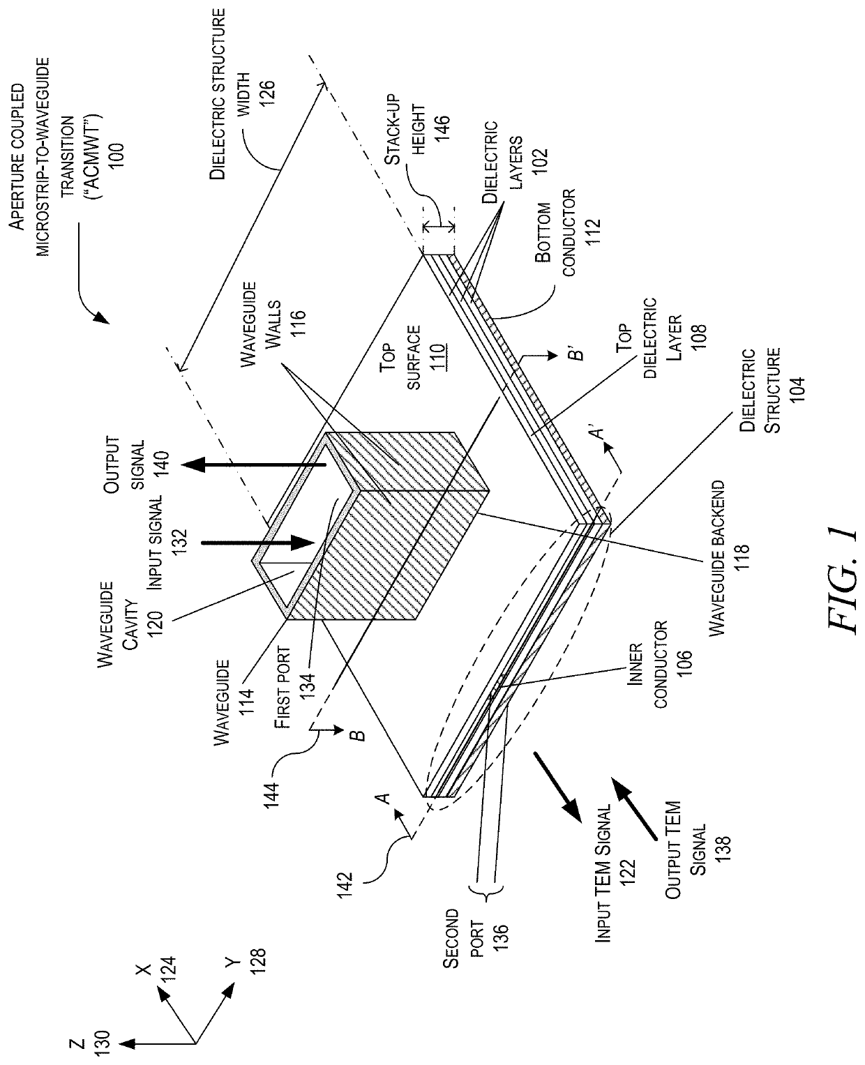
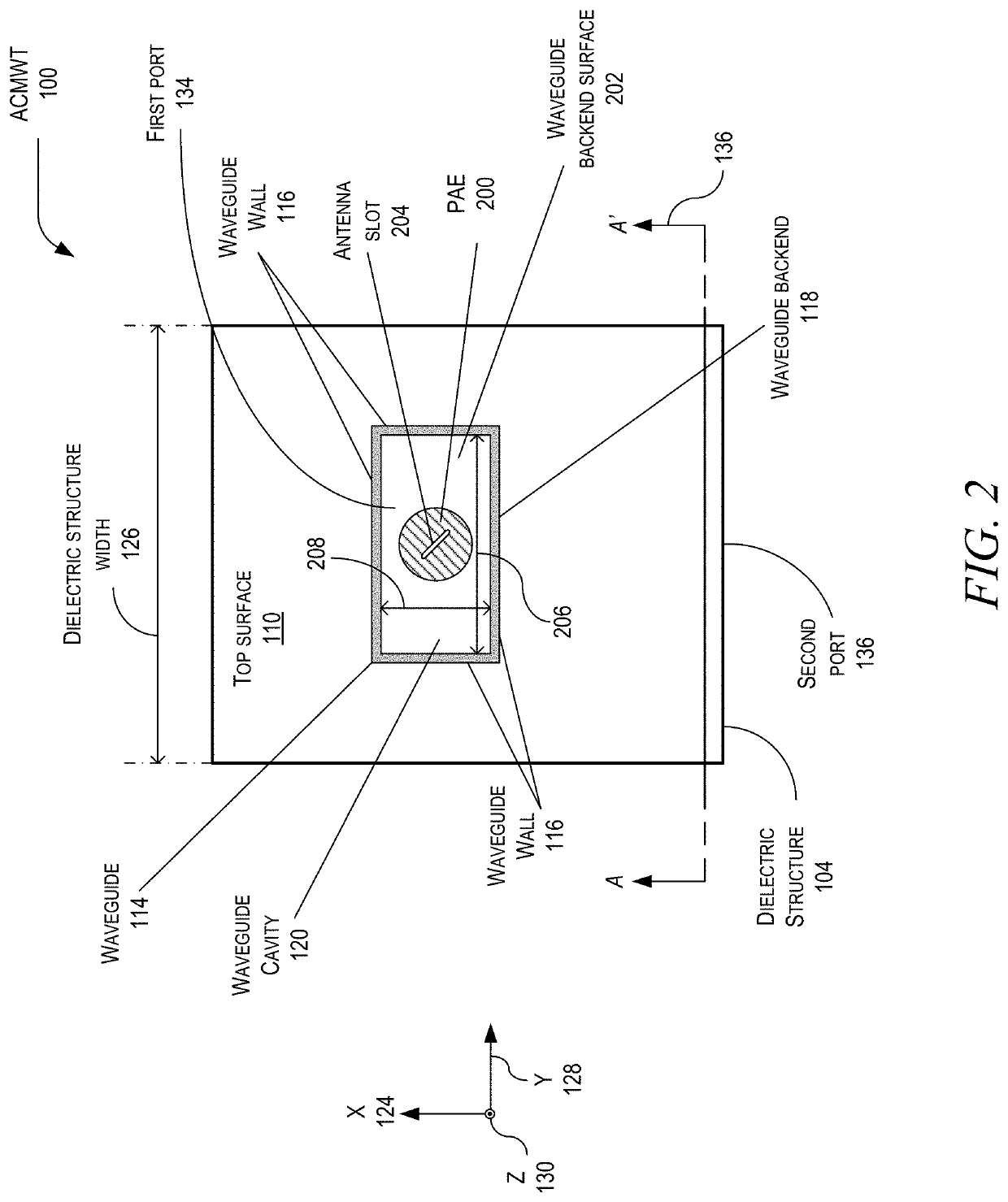
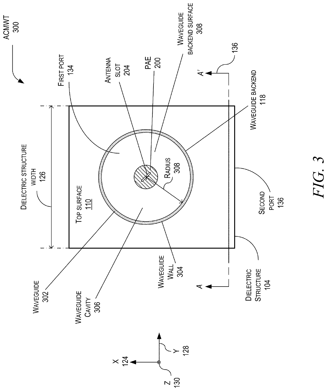
[0047]An aperture coupled microstrip-to-waveguide transition (“ACMWT”) is disclosed. The ACMWT includes a plurality of dielectric layers forming a dielectric structure and an inner conductor formed within the dielectric structure. The plurality of dielectric layers includes a top dielectric layer that has a top surface. The ACMWT further includes a patch antenna element (“PAE”) formed on the top surface, a bottom conductor, an antenna slot within the PAE, a coupling element (“CE”) formed within the dielectric structure between the PAE and inner conductor, and a waveguide. The waveguide includes at least one waveguide wall and a waveguide backend, where the waveguide backend has a waveguide backend surface that is a portion of the top surface of the top dielectric layer and where the waveguide backend surface and the at least one waveguide wall form a waveguide cavity within the waveguide. The PAE is a conductor and is located within the waveguide cavity at the waveguide backend surf...


PUM

PropertyMeasurementUnit
thicknessaaaaaaaaaa
thicknessaaaaaaaaaa
thicknessaaaaaaaaaa

Abstract

An aperture coupled microstrip-to-waveguide transition (“ACMWT”) is disclosed that includes a plurality of dielectric layers forming a dielectric structure and an inner conductor formed within the dielectric structure. The plurality of dielectric layers includes a top dielectric layer that has a top surface. The (“ACMWT”) further includes a patch antenna element (“PAE”) formed on the top surface, a bottom conductor, an antenna slot within the PAE, a coupling element (“CE”) formed above the inner conductor and below the PAE, and a waveguide. The waveguide includes at least one waveguide wall and a waveguide backend, where the waveguide backend has a waveguide backend surface that's a portion of the top surface of the top dielectric layer and where the waveguide backend surface and the at least one waveguide wall form a waveguide cavity within the waveguide. The PAE is a conductor located within the waveguide cavity at the waveguide backend surface.

Description

CROSS-REFERENCE TO RELATED APPLICATIONS[0001]This application is related to U. S. patent application Ser. No. ______, entitled “CONFORMAL ANTENNA WITH ENHANCED CIRCULAR POLARIZATION,” filed on August ______, 2018, to inventor John E. Rogers, and U.S. patent application Ser. No. ______, entitled “WAVEGUIDE-FED PLANAR ANTENNA ARRAY WITH ENHANCED CIRCULAR POLARIZATION,” filed on August ______, 2018, to inventor John E. Rogers, both of which applications are incorporated by reference herein in their entireties.BACKGROUND1. Field[0002]The present disclosure is related to waveguide transitions, and more specifically, to microstrip-to-waveguide transitions.2. Related Art[0003]At present, waveguides are used in many RF applications for low-loss signal propagation; however, they are generally not directly compatible with surface-mount device (“SMD”) RF electronics. Known approaches are to utilize waveguide-to-coax adapters for first transitioning from a waveguide to the electronics-compatibl...

Claims


Application Information

Patent Timeline
Patent Type & Authority Applications(United States)
IPC IPC(8): H01P5/08H01P3/08H01P3/12H01P11/00
CPCH01P11/002H01P3/08H01P5/085H01P3/12H01P11/003H01P5/107H01Q9/0414H01Q13/06H01Q21/0075H01Q9/045H01Q21/065
Inventor ROGERS, JOHN E.
Owner THE BOEING CO
Why Eureka
Try Eureka