Light-emitting device and method of manufacturing the same

a technology of light-emitting devices and manufacturing methods, which is applied in the direction of lighting and heating apparatus, instruments, lenses, etc., can solve the problems of increased lens size, increased light-emitting device size, and uneven illuminance distribution, so as to reduce the unevenness of emission color and small size , the effect of small siz

Active Publication Date: 2020-03-05
NICHIA CORP
View PDF0 Cites 8 Cited by
  • Summary
  • Abstract
  • Description
  • Claims
  • Application Information

AI Technical Summary

Benefits of technology

[0004]When the number of light-emitting elements in a light-emitting device is increased so as to increase the output power, the size of a lens is increased, which leads to increase in size of the light-emitting device. Therefore, in order to miniaturize the device without changing the number of light-emitting elements and the size of the lens, reduction in the distance between the light-emitting elements is considered. However, reduction in the distance between the light-emitting elements may cause unevenness in the illuminance distribution. In particular, reduction in the distance between the light-emitting elements that emit different colors may cause unevenness in emission color when the light-emitting elements are turned on at the same time.
[0005]Certain embodiments according to the present disclosure allow for obtaining a light-emitting device with small size in which unevenness in emission color is reduced, and a method of manufacturing the light-emitting device.
[0009]According to certain embodiments of the present disclosure, it is possible to obtain a light-emitting device of a small size in which unevenness in emission color is reduced. According to certain embodiments of the present disclosure, it is possible to manufacture a light-emitting device of a small size in which unevenness in emission color is reduced.

Problems solved by technology

When the number of light-emitting elements in a light-emitting device is increased so as to increase the output power, the size of a lens is increased, which leads to increase in size of the light-emitting device.
However, reduction in the distance between the light-emitting elements may cause unevenness in the illuminance distribution.
In particular, reduction in the distance between the light-emitting elements that emit different colors may cause unevenness in emission color when the light-emitting elements are turned on at the same time.

Method used


Image

  • Light-emitting device and method of manufacturing the same
  • Light-emitting device and method of manufacturing the same
  • Light-emitting device and method of manufacturing the same

Examples


first embodiment

Configuration of Light-Emitting Device

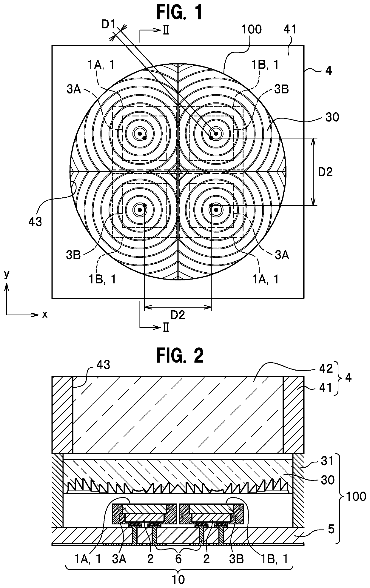
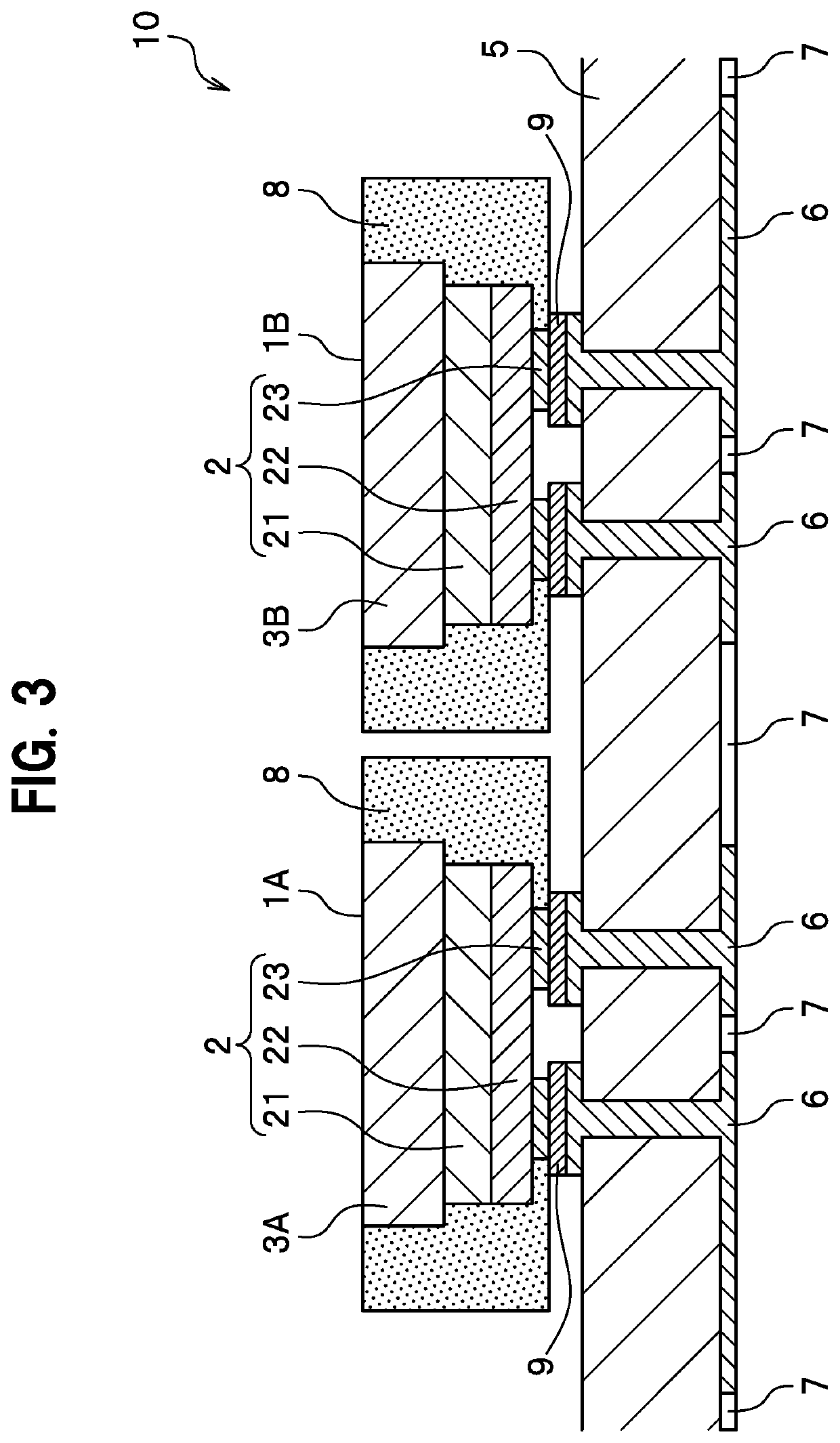
[0025]A configuration of a light-emitting device according to a first embodiment of the present invention is described with reference to FIGS. 1 to 3. FIG. 1 is a schematic plan view showing the configuration of the light-emitting device according to the first embodiment. FIG. 2 is a schematic sectional view taken along the line II-II in FIG. 1. FIG. 3 is a schematic sectional view showing an example of a configuration of a light source device shown in FIG. 2.

[0026]A light-emitting device 100 constitutes, for example, a flash module for a camera. The light-emitting device 100 is incorporated in a housing 4 of a smartphone, a tablet terminal or the like. The housing 4 includes a main body 41 made of, for example, stainless steel, and a cover glass 42 covering the light-emitting device 100 incorporated in the housing 4. The cover glass 42 is disposed in a through hole 43 of the main body 41. FIG. 1 shows a portion of the light-emitting device that...

second embodiment

[0079]FIG. 12 is a plan view schematically showing a configuration of a light-emitting device according to a second embodiment. As shown in FIG. 12, a light-emitting device 100C according to the second embodiment includes a different number of light-emitting elements and a different shape of compound eye lens from those of the light-emitting device 100 according to the first embodiment. Hereinafter, the same reference numerals indicate the same or similar components as those of the light-emitting device 100 shown in FIG. 1, and duplicative description thereof will be omitted. In FIG. 12, illustration of a housing 4 is omitted, and a portion of the light-emitting device that can be seen through a cover glass 42 attached to a through hole 43 of a main body 41 is shown.

[0080]The light-emitting device 100C includes a light source device 10 including a plurality of light-emitting elements 1 arranged in an array on a base member 5 (see FIG. 2), and a compound eye lens 30C. The compound ey...


PUM

PropertyMeasurementUnit
distanceaaaaaaaaaa
dominant wavelengthaaaaaaaaaa
transmittanceaaaaaaaaaa

Abstract

A light-emitting device includes: a plurality of light-emitting elements arranged in an array on a base member; and a compound eye lens that includes a plurality of lens parts disposed above the base member and facing the plurality of light-emitting elements. The plurality of light-emitting elements are arranged such that each of the plurality of light-emitting elements faces a corresponding one of the lens parts, and a center of each of the plurality of light-emitting elements is offset from a lens center of the corresponding one of the lens parts of the compound eye lens in a direction toward a center of the compound eye lens in a plan view. The plurality of light-emitting elements include first light-emitting elements and second light-emitting elements that are alternately arranged, wherein an emission color of the first light-emitting elements is different from an emission color of the second light-emitting elements.

Description

CROSS-REFERENCE TO RELATED APPLICATIONS[0001]This application claims priority to Japanese Patent Application NO. 2018-162681, filed on Aug. 31, 2018, the entire contents of which are incorporated herein by reference.BACKGROUND OF THE INVENTION[0002]The present disclosure relates to a light-emitting device and a method of manufacturing the same.[0003]Known light-emitting devices used for a flash for camera, etc., include a plurality of light-emitting elements, and a plurality of lenses, each combined with a respective one of the plurality of the light-emitting elements (for example, see Japanese Patent Application Publication NO. 2016-224394).SUMMARY[0004]When the number of light-emitting elements in a light-emitting device is increased so as to increase the output power, the size of a lens is increased, which leads to increase in size of the light-emitting device. Therefore, in order to miniaturize the device without changing the number of light-emitting elements and the size of the...

Claims


Application Information

Patent Timeline
Patent Type & Authority Applications(United States)
IPC IPC(8): G03B15/05G02B3/08
CPCG02B3/08G03B2215/0589G03B15/05G02B3/0056G02B19/0066G02B19/0014G03B2215/0592G03B15/02F21V5/007F21V9/30F21V5/045
Inventor OKAHISA, TSUYOSHIMATSUOKA, SHINYA
Owner NICHIA CORP
Why Eureka
Try Eureka