Touch sensor and image display device including the same

a technology of image display device and touch sensor, which is applied in the direction of instruments, computing, electric digital data processing, etc., can solve the problems of failure to conceive the parasitic capacitance within the electrodes of the touch sensor, image quality deterioration, etc., and achieve the effect of avoiding or reducing parasitic capacitance, reducing the width of the extension portion overlapping the connecting portion, and preventing sensitivity degradation of the touch sensor

Active Publication Date: 2020-03-19
DONGWOO FINE CHEM CO LTD
View PDF7 Cites 7 Cited by
  • Summary
  • Abstract
  • Description
  • Claims
  • Application Information

AI Technical Summary

Benefits of technology

[0026]In a touch sensor according to exemplary embodiments as described above, a bridge electrode may include an extension portion having a width smaller than that of both end portions of the bridge electrode, and the extension portion may overlap a connecting portion that may be integral with sensing electrodes. The width of the extension portion overlapping the connecting portion may be reduced so that a parasitic capacitance may be avoided or reduced and a sensitivity degradation of the touch sensor may be prevented. The connecting portion may include an etched region so that the parasitic capacitance may be suppressed more efficiently.
[0027]Additionally, areas of the bridge electrode and the connecting portion may be decreased so that a visibility of electrodes and a color sense difference due to a reflectivity change may be prevented.

Problems solved by technology

Further, a visibility of electrodes may be increased by the connecting patterns, and an image quality of an image display device may be also deteriorated.
For example, Korean Registered Patent No. 10-1315227 describes structures for reducing capacitance generated between a touch sensor and a data line, however, fails to conceive the parasitic capacitance within electrodes of the touch sensor.

Method used


Image

  • Touch sensor and image display device including the same
  • Touch sensor and image display device including the same
  • Touch sensor and image display device including the same

Examples


experimental example

tivity and Chromaticity

[0100]FIG. 9 is a top planar view illustrating positions for measuring reflectivity and chrominance in accordance with Experimental Example.

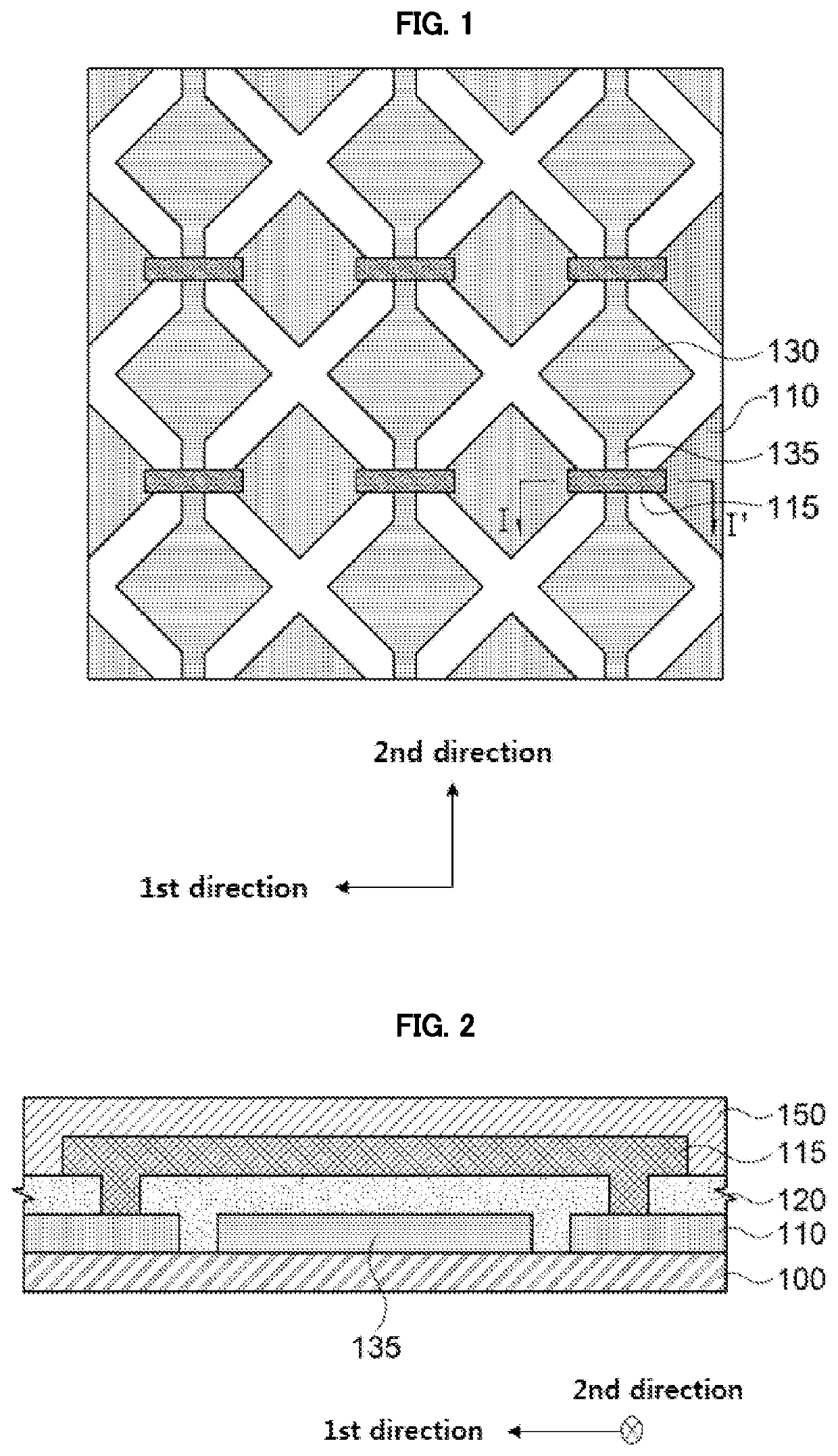
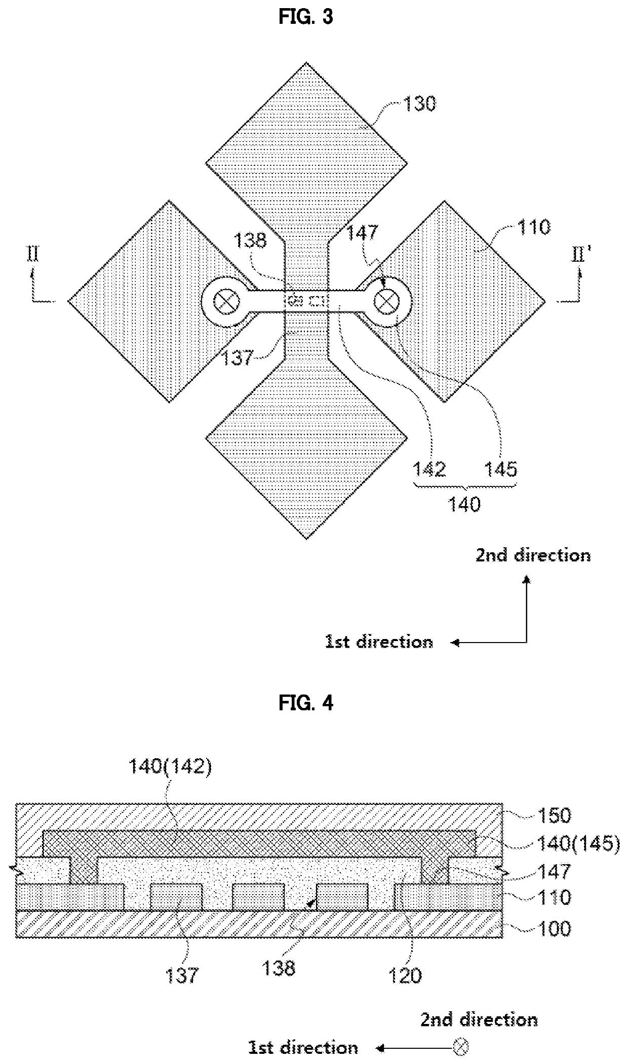
[0101]Specifically, ITO was deposited on a COP substrate, and then patterned to form the first sensing electrode 110, the second sensing electrode 130 and the connecting portion 137 (for convenience of explanation, an illustration of the second sensing electrode 130 is omitted in FIG. 9), each thickness of which was 450 Å. The etched regions 138 each having a hole shape with a dimension of 16 μm×80 μm were formed in the connecting portion 137.

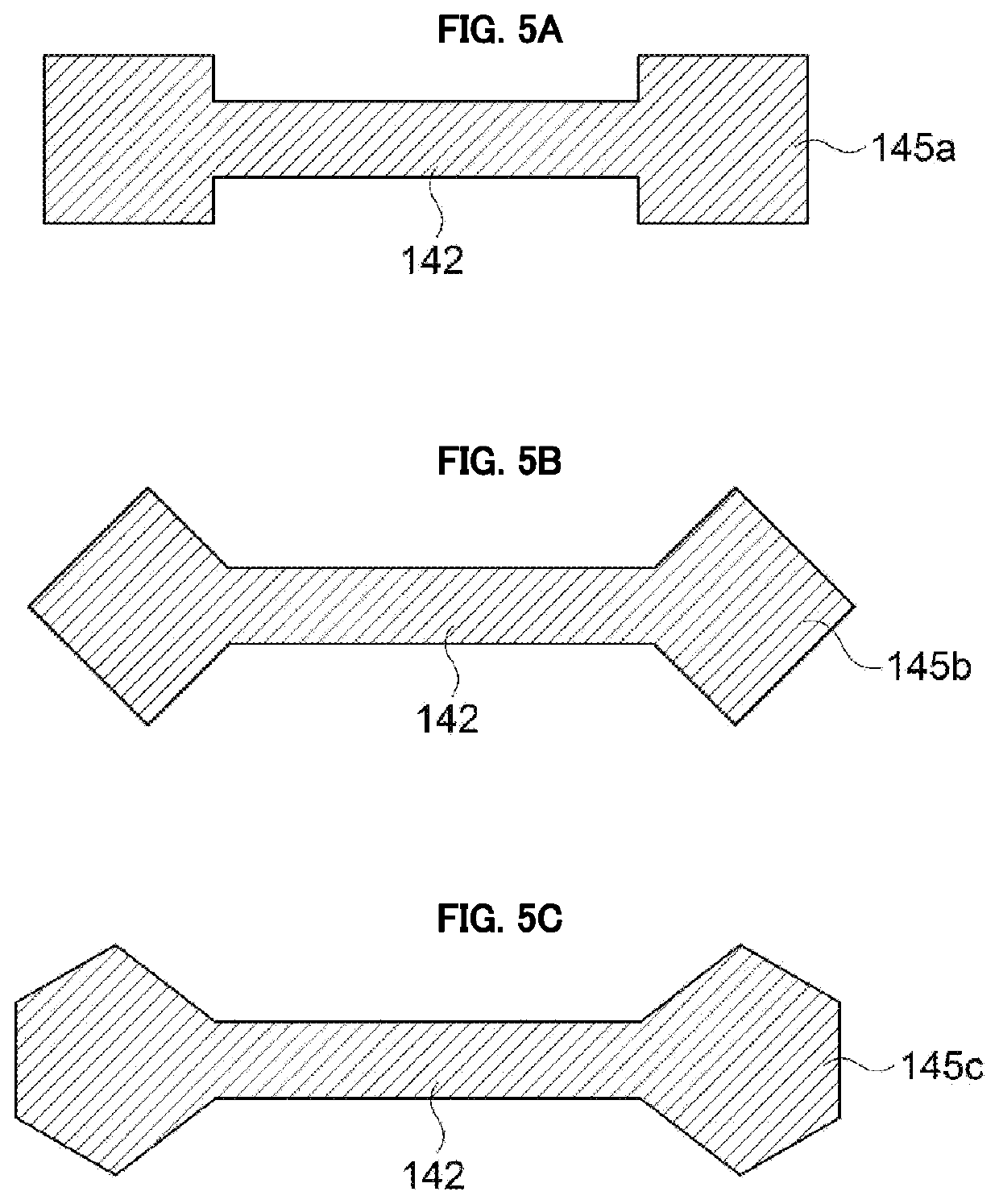
[0102]An acryl-based resin was coated on the first sensing electrodes 110, the second sensing electrode 130 and the connecting portion 137 to form an insulation layer (not illustrated), and an ITO layer was deposited on the insulation layer and etched to form the bridge electrode 140 (thickness: 1250 A) including the extension portion 142 and the expanded portion 145.

[0103]Specificall...


PUM

PropertyMeasurementUnit
temperatureaaaaaaaaaa
thicknessaaaaaaaaaa
diameteraaaaaaaaaa

Abstract

A touch sensor includes a base layer, sensing electrodes arranged on the base layer, a bridge electrode and a connecting portion. The sensing electrode layer includes first sensing electrodes arranged along a first direction parallel to a top surface of the base layer, and second sensing electrodes arranged along a second direction parallel to the top surface of the base layer. The bridge electrode is disposed on the sensing electrodes to electrically connect the first sensing electrodes neighboring in the first direction to each other. The bridge electrode includes an extension portion and expanded portions formed both ends of the extension portion. The expanded portion has a width greater than that of the extension portion. The connecting portion electrically connects the second sensing electrodes neighboring in the second direction and includes at least one etched region.

Description

CROSS-REFERENCE TO RELATED APPLICATION AND CLAIM OF PRIORITY[0001]This application claims priority to Korean Patent Application No. 10-2018-0110713 filed on Sep. 17, 2018 in the Korean Intellectual Property Office (KIPO), the entire disclosure of which is incorporated by reference herein.BACKGROUND1. Field[0002]The present invention relates to a touch sensor and an image display device including the same. More particularly, the present invention relates to a touch sensor including a plurality of sensing electrodes and conductive patterns and an image display device including the same.2. Description of the Related Art[0003]As information technologies are being developed, various demands in display devices having thinner dimension, light-weight, high efficiency in power consumption, etc., are increasing. The display device may include a flat panel display device such as a liquid crystal display (LCD) device, a plasma display panel (PDP) device, an electro-luminescent display device, a...

Claims


Application Information

Patent Timeline
Patent Type & Authority Applications(United States)
IPC IPC(8): G06F3/044G06F3/041
CPCG06F2203/04112G06F3/0416G06F3/044G06F3/0412G06F2203/04103G06F2203/04111G06F3/0443G06F3/0445
Inventor KWON, DO HYOUNGNOH, SUNG JINRYU, HAN TAEPARK, SANG JINLEE, JUN GU
Owner DONGWOO FINE CHEM CO LTD
Why Eureka
Try Eureka