Semiconductor device
a technology of silicon and power devices, applied in the direction of semiconductor devices, electrical devices, transistors, etc., can solve the problems of difficult to achieve higher performance, limited operation range of power devices including silicon at high temperature, and reaching the limit of silicon performance, etc., to achieve high driving voltage, large current, and high temperature operation
- Summary
- Abstract
- Description
- Claims
- Application Information
AI Technical Summary
Benefits of technology
Problems solved by technology
Method used
Image

Examples
embodiment 1
[0067]In this embodiment, a structural example of a semiconductor device of one embodiment of the present invention is described with reference to drawings. Here, a transistor is described as an example of the semiconductor device.
Structural Example 1
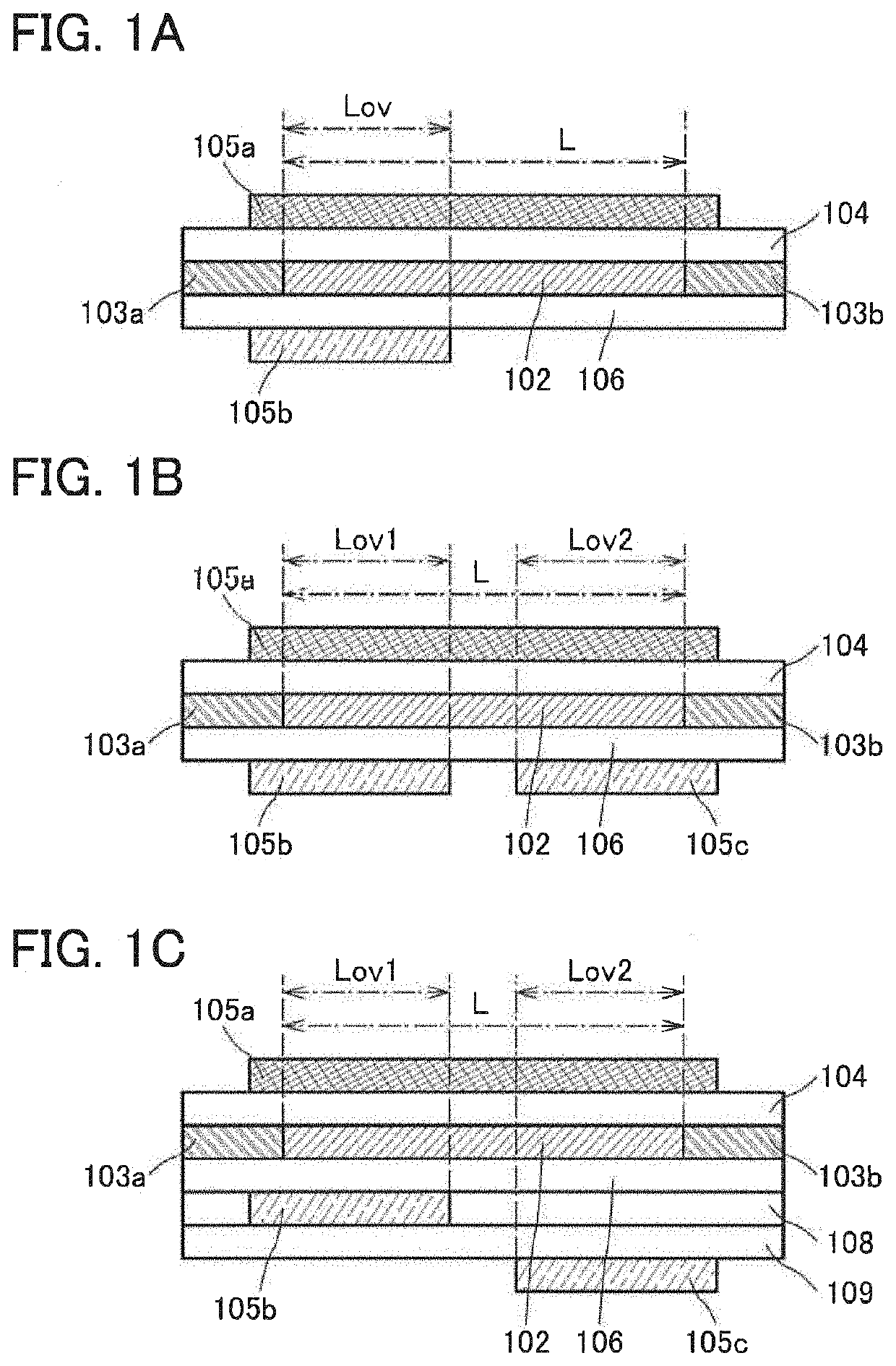
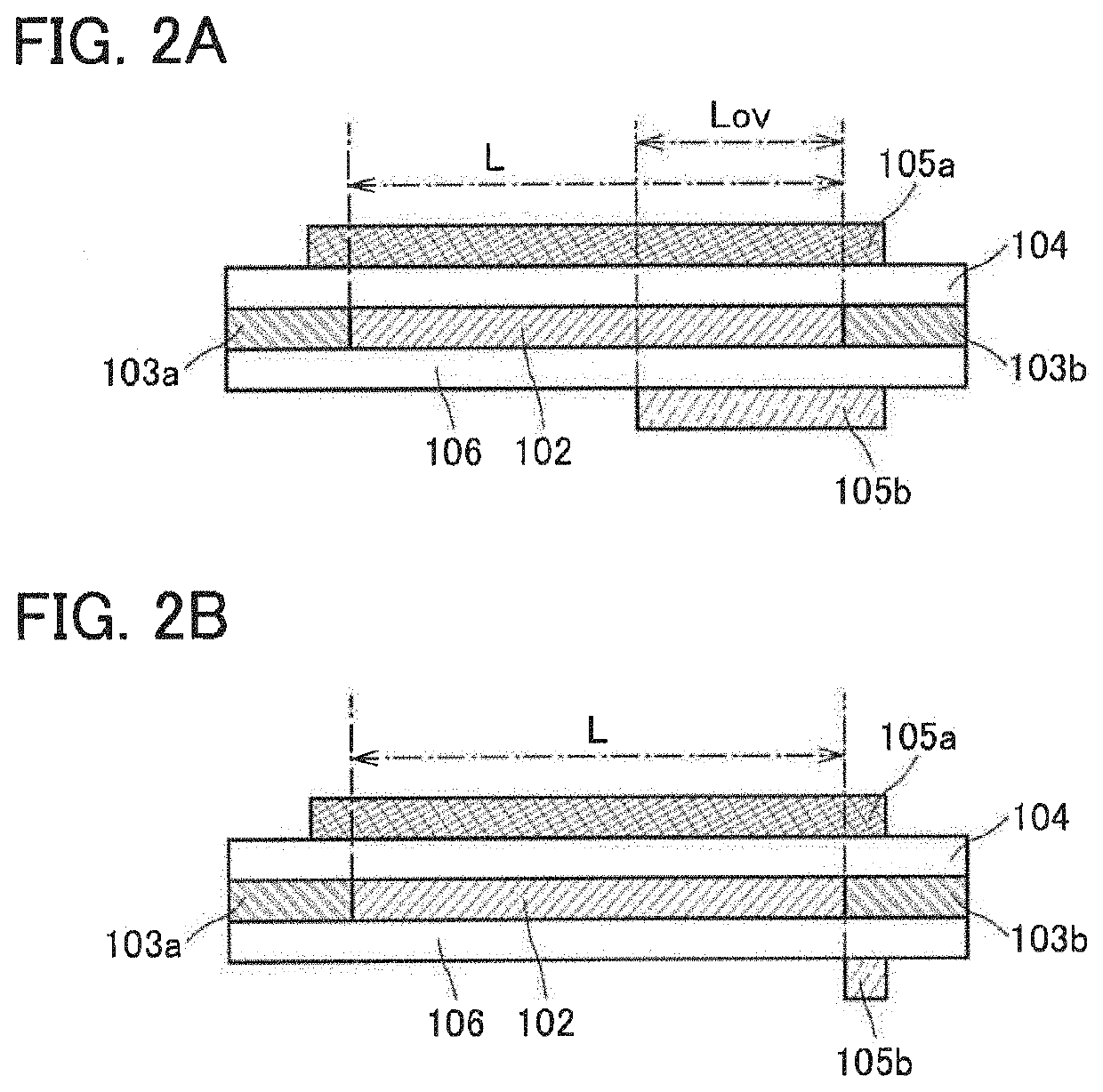
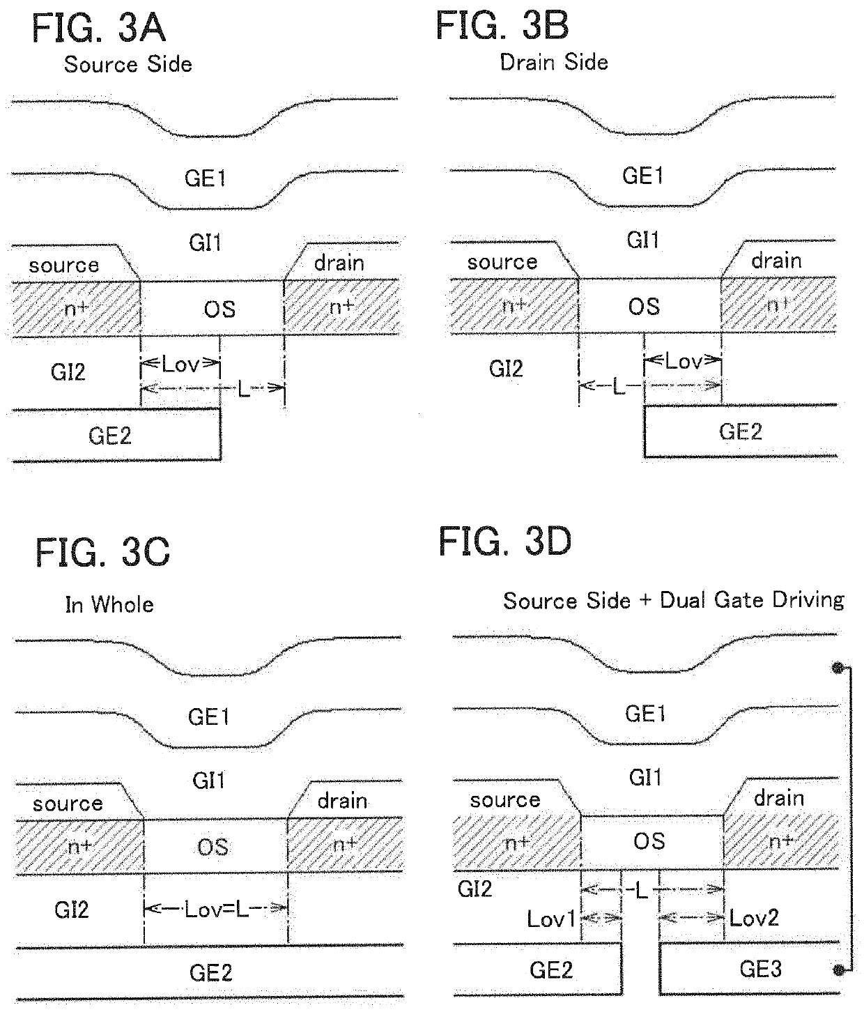
[0068]FIGS. 1A to 1C are schematic cross-sectional views in the channel length direction each for illustrating a positional relationship between typical components in a structural example of a transistor of one embodiment of the present invention.
[0069]A transistor in FIG. 1A includes a semiconductor layer 102, a first electrode 103a and a second electrode 103b which are electrically connected to the semiconductor layer 102, a first gate electrode 105a overlapping with the semiconductor layer 102 with an insulating layer 104 therebetween, and a second gate electrode 105b provided to oppose the first gate electrode 105a with the semiconductor layer 102 therebetween and overlapping with part of the semiconductor layer 102 with an insulati...
embodiment 2
[0182]In this embodiment, specific structural examples of a semiconductor device of one embodiment of the present invention and a manufacturing method example thereof are described with reference to drawings. Here, a transistor is described as an example of the semiconductor device. Note that portions similar to those described above are not described in some cases.
Structural Example
[0183]FIG. 15A is a schematic top view of a transistor 100 described in this structural example FIG. 15B is a schematic cross-sectional view taken along line A-B in FIG. 15A, and FIG. 15C is a schematic cross-sectional view taken along line C-D in FIG. 15A. Some components are not illustrated in FIG. 15A for clarity.
[0184]The transistor 100 provided over a substrate 101 includes an island-shaped semiconductor layer 102, a first electrode 103a and a second electrode 103b each electrically connected to the semiconductor layer 102, a first gate electrode 105a and a second gate electrode 105b each overlappin...
modification example
[0221]Structural Examples of a transistor that are partly different from the structure of the transistor 100 are described below. Note that description of the portions already described is omitted and different portions are described in detail. Even when positions and shapes of components are different from those in the above example, the same reference numerals are used as long as the components have the same functions as those in the above example, and detailed description thereof is omitted in some cases.
PUM
| Property | Measurement | Unit |
|---|---|---|
| drain voltage Vd | aaaaa | aaaaa |
| drain voltage Vd | aaaaa | aaaaa |
| threshold voltage | aaaaa | aaaaa |
Abstract
Description
Claims
Application Information
 - R&D Engineer
- R&D Manager
- IP Professional
- Industry Leading Data Capabilities
- Powerful AI technology
- Patent DNA Extraction
Browse by: Latest US Patents, China's latest patents, Technical Efficacy Thesaurus, Application Domain, Technology Topic.
© 2024 PatSnap. All rights reserved.Legal|Privacy policy|Modern Slavery Act Transparency Statement|Sitemap