TFT pixel threshold voltage compensation circuit with short one horizontal time

a threshold voltage and compensation circuit technology, applied in the field of electronic circuit design and operation, can solve problems such as difficulty in further reducing without degrading compensation accuracy

Active Publication Date: 2020-04-30
SHARP KK
View PDF0 Cites 6 Cited by
  • Summary
  • Abstract
  • Description
  • Claims
  • Application Information

AI Technical Summary

Benefits of technology

[0011]The present invention relates to pixel circuits that are capable of compensating the threshold voltage variations of the drive transistor with an ultra-short one horizontal time 1H of less than about 2 μs, which is shorter as compared to conventional configurations, with additionally removing the possible memory effects associated with the OLED device and drive transistor from the previous frame.

Problems solved by technology

The threshold compensation time is decided by the drive transistor characteristics and is difficult to reduce further without degrading the compensation accuracy.

Method used


Image

  • TFT pixel threshold voltage compensation circuit with short one horizontal time
  • TFT pixel threshold voltage compensation circuit with short one horizontal time
  • TFT pixel threshold voltage compensation circuit with short one horizontal time

Examples


Embodiment Construction

[0025]Embodiments of the present invention will now be described with reference to the drawings, wherein like reference numerals are used to refer to like elements throughout. It will be understood that the figures are not necessarily to scale.

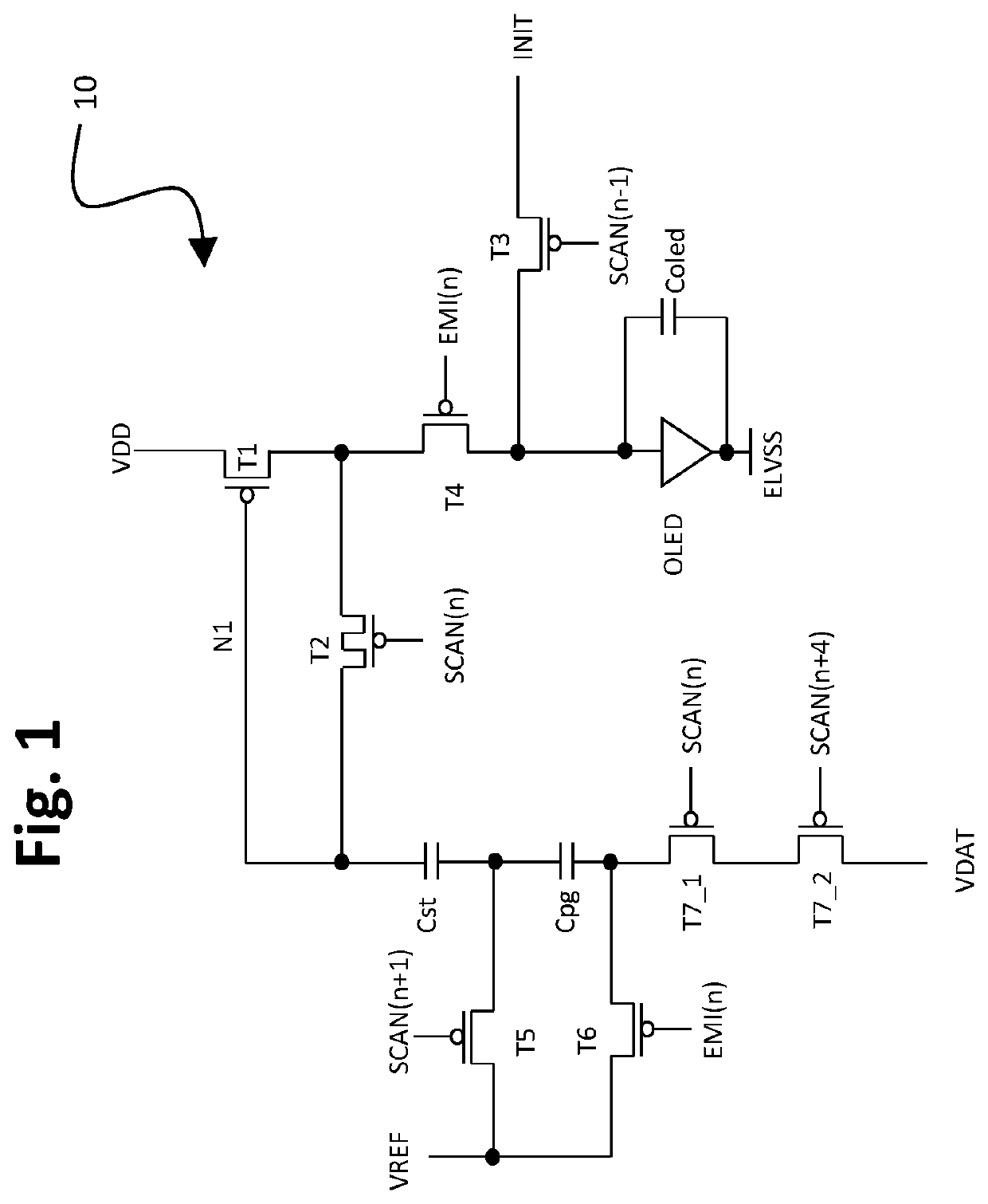
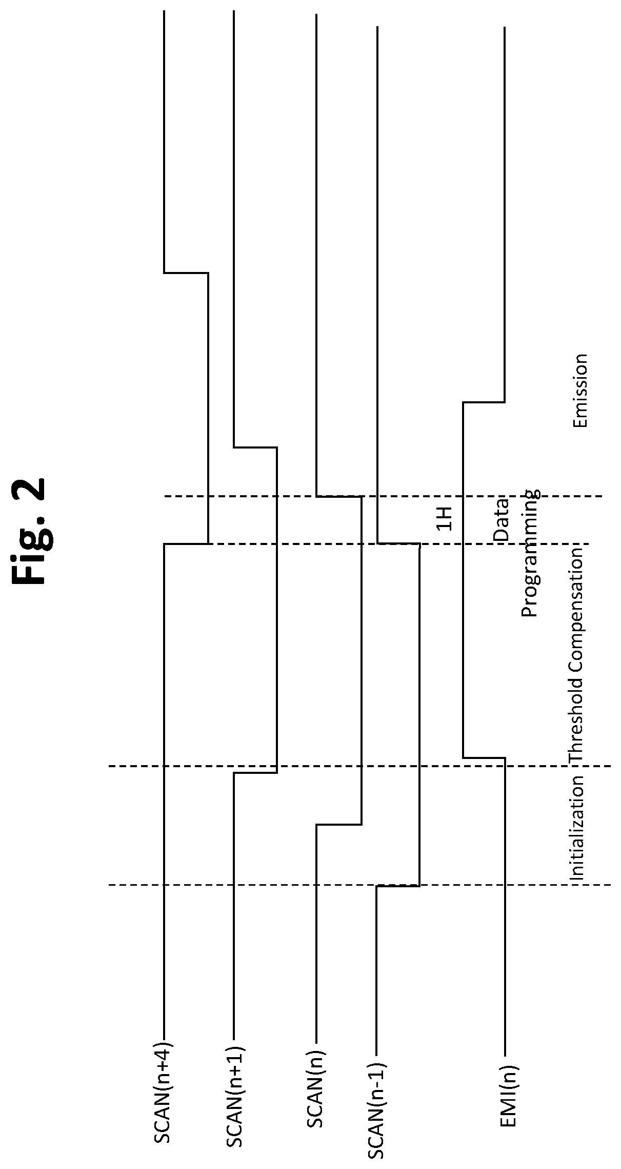
[0026]FIG. 1 is a drawing depicting a first circuit configuration 10 in accordance with embodiments of the present invention, and FIG. 2 is a timing diagram associated with the operation of the circuit configuration 10 of FIG. 1. In this example, the circuit 10 is configured as a TFT circuit that includes multiple p-type transistors T1-T7_2 and two capacitors including a storage Cst and a programming capacitor Cpg. The circuit elements drive a light-emitting device, such as for example an OLED. The light-emitting device (OLED) has an associated internal capacitance, which is represented in the circuit diagram as Coled. In addition, although the embodiments are described principally in connection with an OLED as the light-emitting device, compa...


PUM


Abstract

A pixel circuit includes a drive transistor that controls an amount of current to a light-emitting device, and a second transistor connected to the gate of the drive transistor and a second terminal of the drive transistor, such that when the second transistor is in an on state the drive transistor becomes diode-connected. A threshold voltage of the drive transistor is compensated during a compensation phase while the drive transistor is diode connected. The light-emitting device is connected between the drive transistor and at a second node to a first voltage input. The pixel circuit further includes a storage capacitor having a first plate connected to the gate of the drive transistor, and a programming capacitor having a first plate connected to a second plate of the storage capacitor, and a second plate of the programming capacitor is electrically connected to a data voltage input during a data programming phase. The second plate of the storage capacitor and the first plate of the programming capacitor are connectable to a reference voltage to perform the compensation phase independently of the programming phase, and the storage capacitor and the programming capacitor are series connected during the emission phase.

Description

TECHNICAL FIELD[0001]The present invention relates to design and operation of electronic circuits for delivering electrical current to an element in a display device, such as for example to an organic light-emitting diode (OLED) in the pixel of an active matrix OLED (AMOLED) display device.BACKGROUND ART[0002]Organic light-emitting diodes (OLED) generate light by re-combination of electrons and holes, and emit light when a bias is applied between the anode and cathode such that an electrical current passes between them. The brightness of the light is related to the amount of the current. If there is no current, there will be no light emission, so OLED technology is a type of technology capable of absolute blacks and achieving almost “infinite” contrast ratio between pixels when used in display applications.[0003]Several approaches are taught in the prior art for pixel thin film transistor (TFT) circuits to deliver current to an element of a display device, such as for example an org...

Claims


Application Information

Patent Timeline
Patent Type & Authority Applications(United States)
IPC IPC(8): G09G3/3258G09G3/3233H01L27/12
CPCH01L27/1214G09G3/3258G09G3/3233G09G2300/0819G09G2300/0842G09G2300/0861G09G2320/045
Inventor LU, TONGBROWNLOW, MICHAEL JAMES
Owner SHARP KK
Why Eureka
Try Eureka