Method and apparatus for PCB washing

a technology of printed circuit boards and washing machines, applied in the field of methods and equipment, can solve the problems of increased material costs, increased rejection costs, and increased rejection costs, and achieve the effect of reducing rejection and wastag

Active Publication Date: 2020-05-28
ROKKO SYST PTE LTD
View PDF3 Cites 1 Cited by
  • Summary
  • Abstract
  • Description
  • Claims
  • Application Information

AI Technical Summary

Benefits of technology

[0006]Consequently, the invention provides for both sides of a PCB to be washed and deburred, reducing rejection and wastage.

Problems solved by technology

In the processing of printed circuit boards (PCBs) being more complex devices, waste through rejection becomes a more expensive issue than the rejection of an integrated circuit having gone through a limited number of processing steps.
For the printed circuit board the larger material costs is clearly an issue but further having more processes to build the PCBs up to the stage of later processing involves a longer manufacturing path and so rejection consequently represents a greater cost.
One aspect of rejection of a PCB is the damage caused by both sawing of the PCB as well as detritus from the sawing process interfering or damaging with such a unit.

Method used


Image

  • Method and apparatus for PCB washing
  • Method and apparatus for PCB washing
  • Method and apparatus for PCB washing

Examples


Embodiment Construction

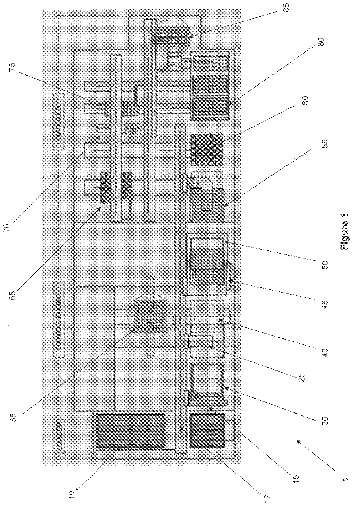
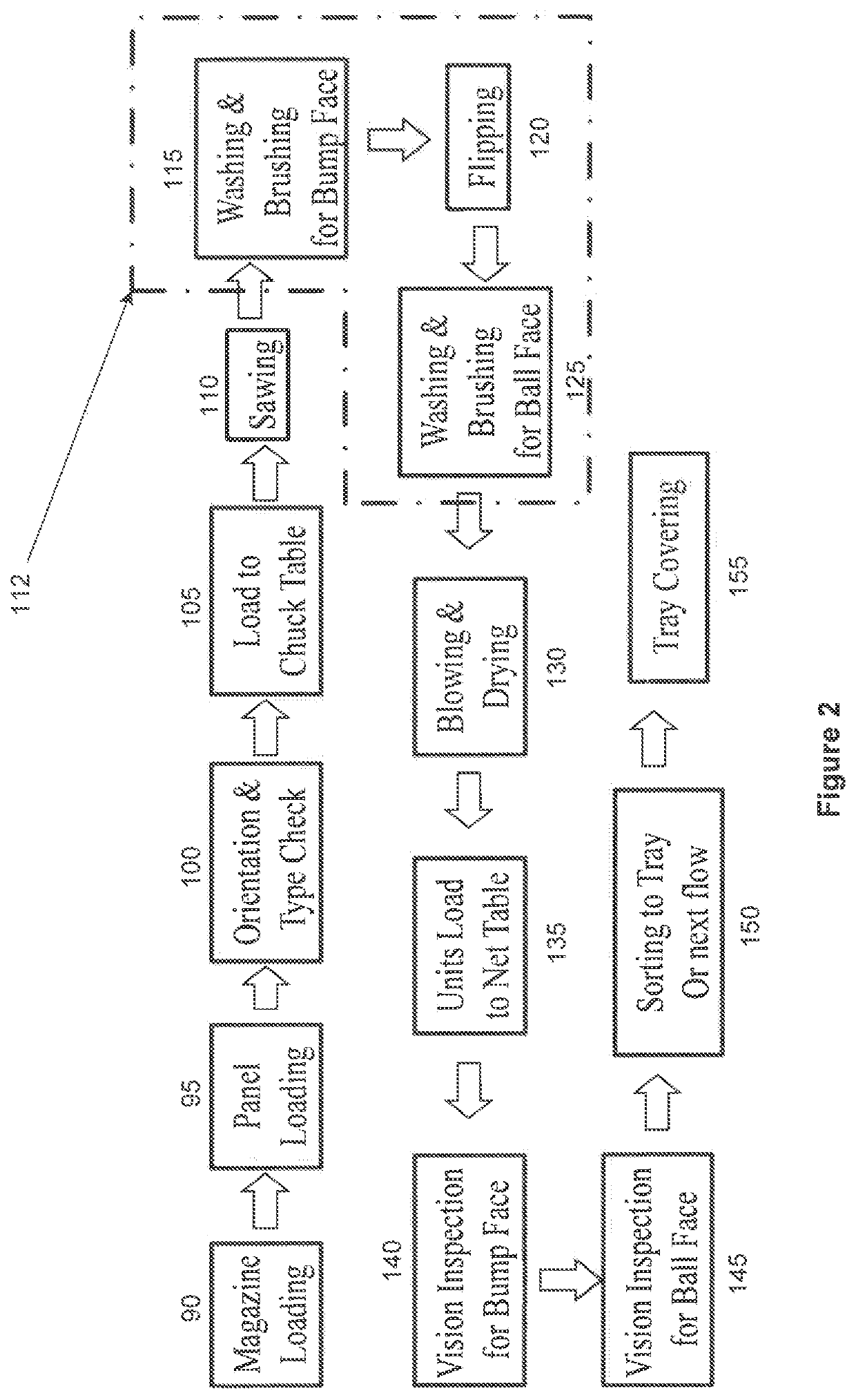
[0019]FIGS. 1 and 2 show a sawing and sorting device for PCBs. Here the device 5 includes a panel magazine 10, 90 for loading 95 PCB substrates into a loading station 20. The PCBs have been manufactured in large single panel with the device 5 arranged to dice the PCBs into separate units.

[0020]The PCB panels are loaded 95 by a pusher (not shown) onto a platform for inspection 100 by inspection device 15 running along a slide 17. The inspection checks the panel for orientation and other data so as to enter into the control system certain parameters such as the type of PCB, panel size, PCB size etc., for eventual use during sawing.

[0021]Once inspected, the panel is loaded 105 to a chuck table 40 by a panel engagement arm 25 running along the aforementioned slide 17. The panel is placed within the sawing zone 35 where a pair of saws dice 110 the panel into separate PCB units. In this embodiment the pair of saws is oriented along a common axis. Once the cut in the panel along that axis ...


PUM


Abstract

A method for washing a plurality of PCB units, the method comprising the steps of: receiving a plurality of PCB units, said PCB units arranged with a bump face projecting downwards; washing the bump face of the PCB units, then; flipping the PCB units as to project a ball face downwards, then; washing the ball face.

Description

FIELD OF THE INVENTION[0001]The invention relates to the processing of printed circuit boards (PCB's). In particular it relates to the separation of a PCB from a panel and subsequent processing.BACKGROUND[0002]In the processing of printed circuit boards (PCBs) being more complex devices, waste through rejection becomes a more expensive issue than the rejection of an integrated circuit having gone through a limited number of processing steps. For the printed circuit board the larger material costs is clearly an issue but further having more processes to build the PCBs up to the stage of later processing involves a longer manufacturing path and so rejection consequently represents a greater cost.[0003]One aspect of rejection of a PCB is the damage caused by both sawing of the PCB as well as detritus from the sawing process interfering or damaging with such a unit. Given the higher cost during to rejection for a PCB, it is therefore important that during the sawing process such sources...

Claims


Application Information

Patent Timeline
Patent Type & Authority Applications(United States)
IPC IPC(8): H05K3/26H05K3/22H05K3/00
CPCH05K3/0052H05K2203/0228H05K2203/0766H05K2203/1563H05K3/227H05K3/26H05K13/0015H05K3/0008H05K3/3436H05K2203/1554H05K2203/0736H05K2203/0756H05K2203/088B24B9/04D06F33/06H05K3/0055H05K2203/0257H05K2203/0346H05K13/028H05K13/02H05K13/0084H05K13/0061
Inventor SHIN, YUN SUKJUNG, JONG JAEJANG, DEOK CHUN
Owner ROKKO SYST PTE LTD
Why Eureka
Try Eureka