[0009] The invention provides a method for applying rewiring to a panel while compensating for position errors of semiconductor chips in component positions of the panel which shortens the
process duration, reduces rejects and permits higher tolerances in the alignment of the semiconductor chips in rows and columns for the production of a panel.
[0013] As compared with the method described above, this method has the
advantage that it manages with two exposure processes of a
photolithography layer in order to compensate for the position errors of the semiconductor chips. In this case, the second
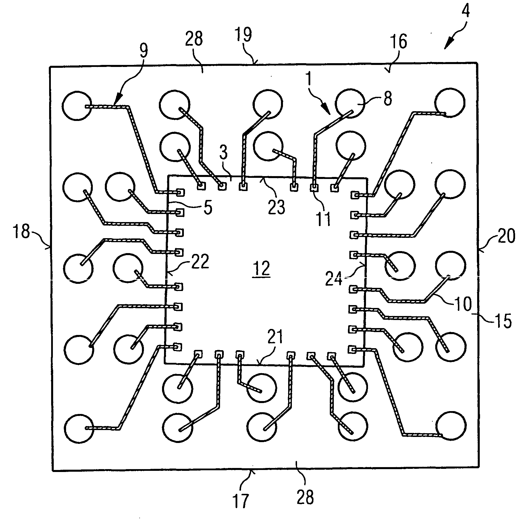
mask having the rewiring lines is positioned in such a way that the rewiring lines of all the contact areas of a component position on the upper sides of the semiconductor chips of the panel meet as accurately as possible. By contrast, the outer contact areas, which are larger than the contact areas, are overlapped by the rewiring lines at arbitrary points, so that a connection is achieved between external contact areas and contact areas by using the two masks, despite position errors of the semiconductor chips.
[0015] Despite a use of a
mask stepper, a fixed and defined pattern of the external contact areas in relation to the rows and columns of the panel is maintained and achieved, so that the aforementioned problems during the application of solder globules and during the division of the panel into individual components are solved by this two-stage exposure with two masks. Furthermore, the
advantage results that, because of the exact alignment of the second mask in relation to the semiconductor
chip and to the contact areas of the semiconductor chip, these contact areas can be made smaller. A reduction in the size of the contact areas, in addition to saving area on the
silicon semiconductor chip, is associated with the possibility of implementing finer step widths or “pitches”, and also a higher rewiring density, since more space becomes possible for conductor tracks between two contact areas.
[0018] For this purpose, firstly optical position registration and evaluation of the position errors of the semiconductor chips in the component positions of the panel are carried out. This is followed, as a second exposure process, by laser structuring of connecting line pieces between the ends of the rewiring lines at the edges of the semiconductor chips and the contact areas on the active upper sides of the semiconductor chips, by means of a laser write beam. This laser structuring for the production of connecting pieces permits a greater position inaccuracy of the semiconductor chips in the individual component positions, since the compensation possibilities provided by a laser write beam, and therefore the compensation of position errors, are improved. The optical laser registration and evaluation of the position errors of the semiconductor chips in the component positions of the panel are used for the purpose of optimizing the alignment of the overall rewiring mask during the first exposure, in such a way that the smallest average distance between the ends of the rewiring lines and the contact areas on the active upper sides of the semiconductor chips is achieved. As a result, the writing period of the laser write beam is optimized and reduced, and therefore the process costs are minimized.
[0019] In this case, too, a constant grid for the external contact areas and therefore for the external housing contour is achieved with the overall rewiring mask. A further
advantage is that, depending on the implementation of the writing geometry of the laser beam, position errors of different size of the chip can be evened out and compensated for. However, on account of the short writing length of the line pieces which still have to be implemented, the method is more cost-effective than complete production of the rewiring structure of the panel by laser structuring by means of a laser write beam.
[0021]
Verification that the method according to the invention has been used for
semiconductor components can be carried out by means of a simple comparison of the rewiring structure which has been produced in accordance with the method of the invention with line structures which have been produced with the aid of conventional methods. In this case, it is characteristic of components which have been produced with a method of the present invention that the external contacts are arranged completely uniformly in a matrix which is aligned in accordance with the edges of the component housing. Furthermore, the line pieces produced by laser writing can be detected at any time because of their uniqueness as a result of connecting rewiring line ends to contact areas on the semiconductor chip. In addition, the characteristic attachment of the rewiring lines to the external contact areas in the case in which a first and a second mask are used can be detected at any time on the components produced.

