Organic light emitting display device

a display device and organic technology, applied in the field of display devices, can solve the problems of shortening the life of the organic light-emitting display devi

Active Publication Date: 2020-07-02
LG DISPLAY CO LTD
View PDF0 Cites 3 Cited by
  • Summary
  • Abstract
  • Description
  • Claims
  • Application Information

AI Technical Summary

Benefits of technology

[0009]An object of the present invention is to provide an organic light emitting display device which has a UV blocking layer provided therein and is thus stable even in environments, such as a UV reliability test or outdoor use for a long time.

Problems solved by technology

An organic light emitting display device is vulnerable to moisture in terms of characteristics of an organic light emitting layer configured to emit light, and an emission area is reduced by UV light and thus does not normally emit light, thus shortening the lifetime of the organic light emitting display device.

Method used


Image

  • Organic light emitting display device
  • Organic light emitting display device
  • Organic light emitting display device

Examples


first embodiment

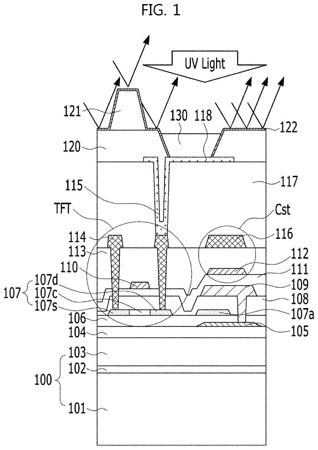
[0049]FIG. 1 is a cross-sectional view of an organic light emitting display device in accordance with the present invention.

[0050]As exemplarily shown in FIG. 1, the organic light emitting display device in accordance with the first embodiment of the present invention includes thin film transistors TFT provided on a substrate, a planarization film 117 covering the thin film transistors TFT except for a part of each thin film transistor, a first electrode 118 connected to the exposed part of the thin film transistor TFT, a bank 120 configured to expose a part of the first electrode 118 to define an emission part, a spacer 121 provided on the bank 120, a UV blocking layer 122 provided on the surfaces of the bank 120 and the spacer 121 except for the upper surface of the first electrode 118 corresponding to the emission part, and an organic light emitting layer 130 overlapping the emission part and the UV blocking layer 122 around the emission part. All the components of the organic li...

second embodiment

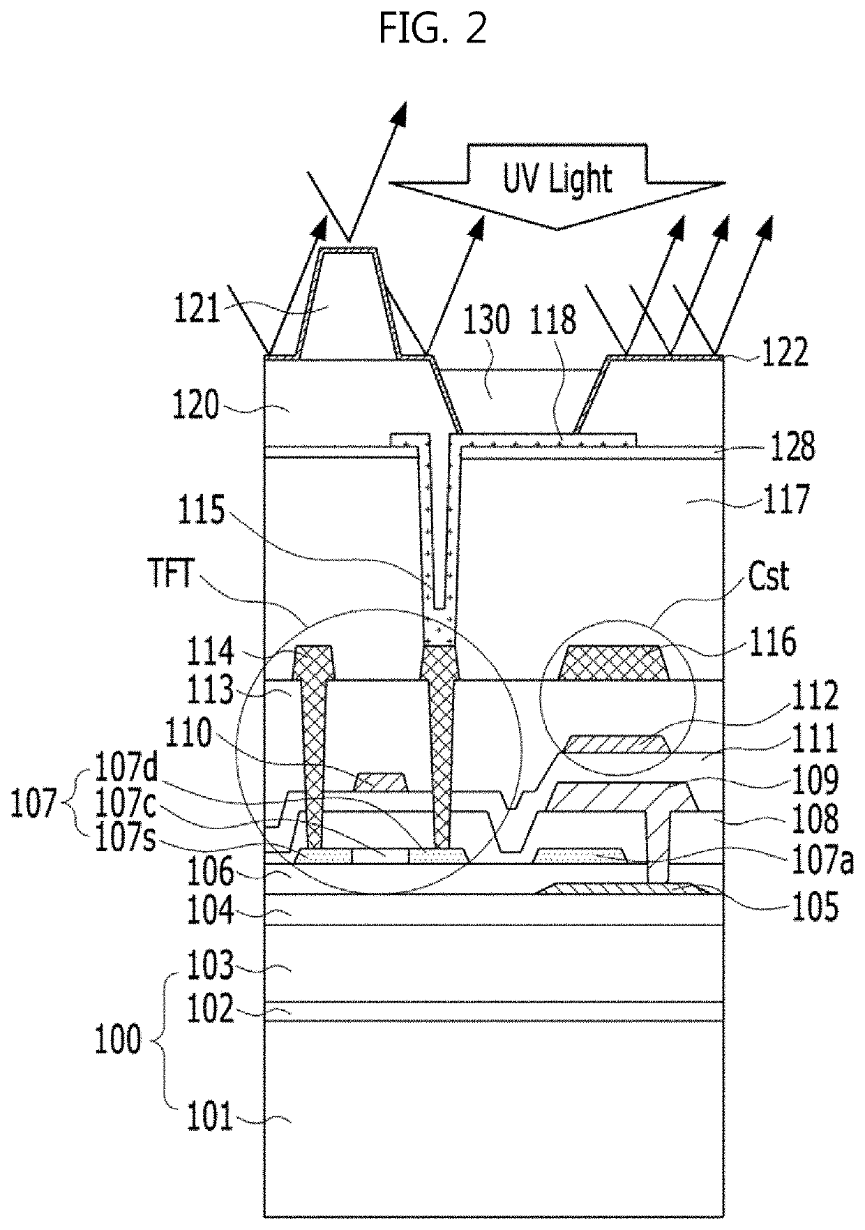
[0086]FIG. 2 is a cross-sectional view of an organic light emitting display device in accordance with the present invention.

[0087]As exemplarily shown in FIG. 2, the organic light emitting display device in accordance with the second embodiment of the present invention further includes an auxiliary UV blocking layer 128 on the upper surface of the planarization film 117 in addition to the structure of the organic light emitting display device in accordance with the first embodiment. The auxiliary UV blocking layer 128 can include a material of the same series as the material of the above-described UV blocking layer 118, i.e., an inorganic blocking film having an excellent UV blocking property, for example, at least one selected from the group consisting of ZnOx, TiOx, SixNy and TaxOy. In case of a top emission type in which the first electrode 118 includes a reflective electrode and the second electrode is a semi-transmissive or transmissive electrode, if the auxiliary UV blocking l...

third embodiment

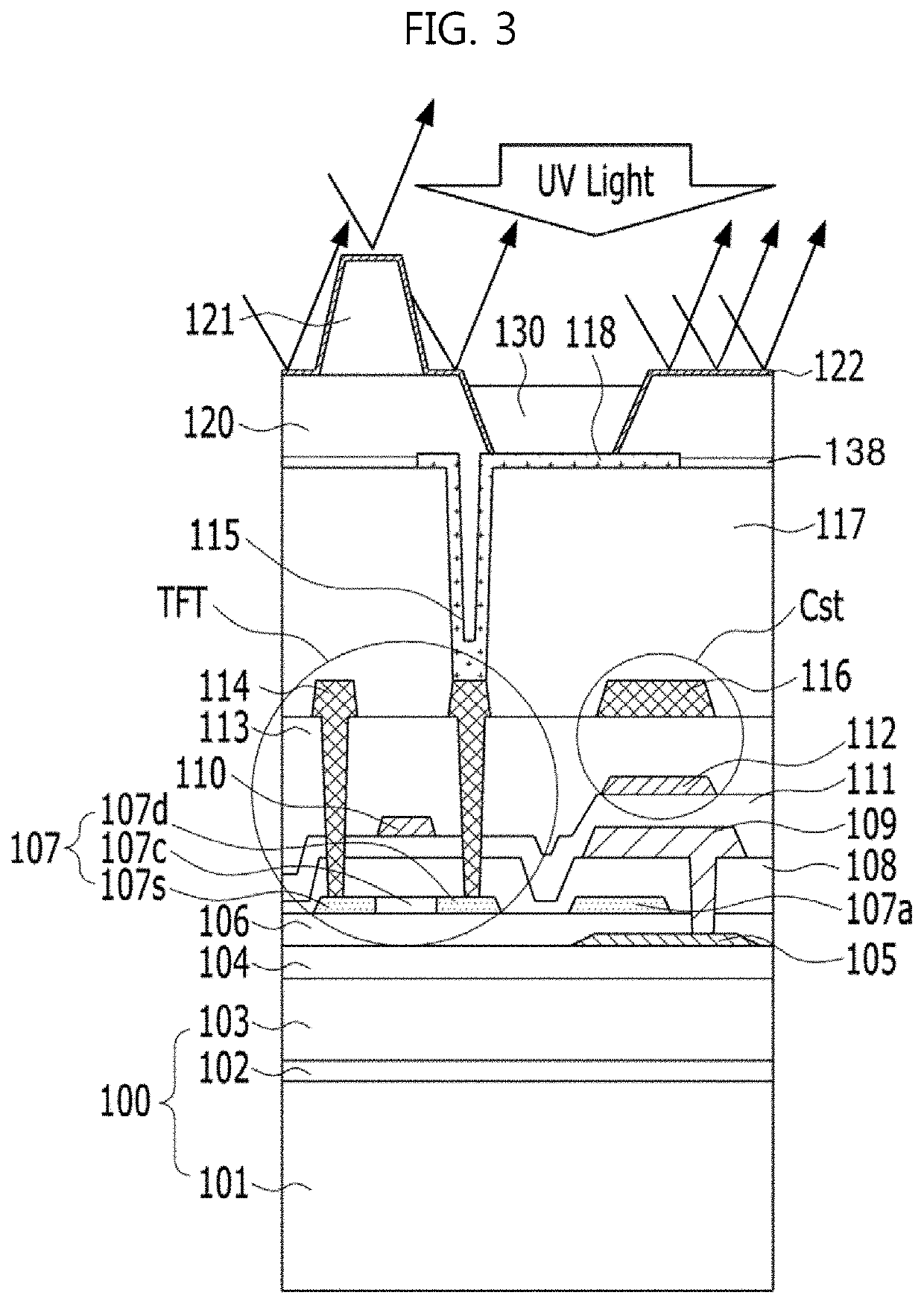
[0089]FIG. 3 is a cross-sectional view of an organic light emitting display device in accordance with the present invention.

[0090]As exemplarily shown in FIG. 3, the third embodiment is a modification of the above-described second embodiment of the present invention, and the organic light emitting display device in accordance with the third embodiment of the present invention can further include an auxiliary UV blocking layer 138 in a region only in which the first electrode 118 is not located. Since the first electrode 118 includes a reflective electrode, as described above, the auxiliary UV blocking layer 138 is provided in a region not provided with the first electrode 118 formed at the outside and, thus, the auxiliary UV blocking layer 138 and the first electrode 118 being coplanar with each other prevents UV light from the top from passing through the auxiliary UV blocking layer 138 and the first electrode 118, thereby blocking UV light.

[0091]FIG. 4 is a cross-sectional view of...


PUM

PropertyMeasurementUnit
wavelengthaaaaaaaaaa
thicknessaaaaaaaaaa
light wavelength bandaaaaaaaaaa

Abstract

Disclosed is an organic light emitting display device using an ultraviolet (UV) blocking film which addresses outgassing from an organic film provided in the display device in environments, such as a UV reliability test or outdoor use for a long time, and addresses degradation of an organic stack in an organic light emitting diode caused by the outgassing.

Description

CROSS-REFERENCE TO RELATED APPLICATION[0001]This application claims the benefit of Korean Patent Application No. 10-2018-0173646, filed on Dec. 31, 2018 in the Korean Intellectual Property Office, the disclosure of which is incorporated herein by reference.BACKGROUND OF THE INVENTIONField of the Invention[0002]The present invention relates to a display device, and more particularly, to an organic light emitting display device which prevents outgassing from an organic film in the display device in environments, such as a UV reliability test or outdoor use for a long time, and prevents degradation of an organic stack in an organic light emitting diode caused by outgassing.Discussion of the Related Art[0003]As we have recently entered the information age, the field of displays which visually display electrical information signals has been rapidly developed and, in order to satisfy such development, various flat display devices having excellent performance, such as thinness, light weigh...

Claims


Application Information

Patent Timeline
Patent Type & Authority Applications(United States)
IPC IPC(8): H01L51/50H01L27/32
CPCH01L27/3206H01L2251/301H01L27/3246H01L51/50H01L27/3258H01L2251/56H01L2227/32H10K59/50H10K59/126H10K59/12H10K59/124H10K59/122H10K50/844H10K59/35H10K50/8428H10K50/856H10K2102/00H10K50/00H10K59/30H10K59/10H10K71/00
Inventor LEE, EUN-HYUNG
Owner LG DISPLAY CO LTD
Why Eureka
Try Eureka