

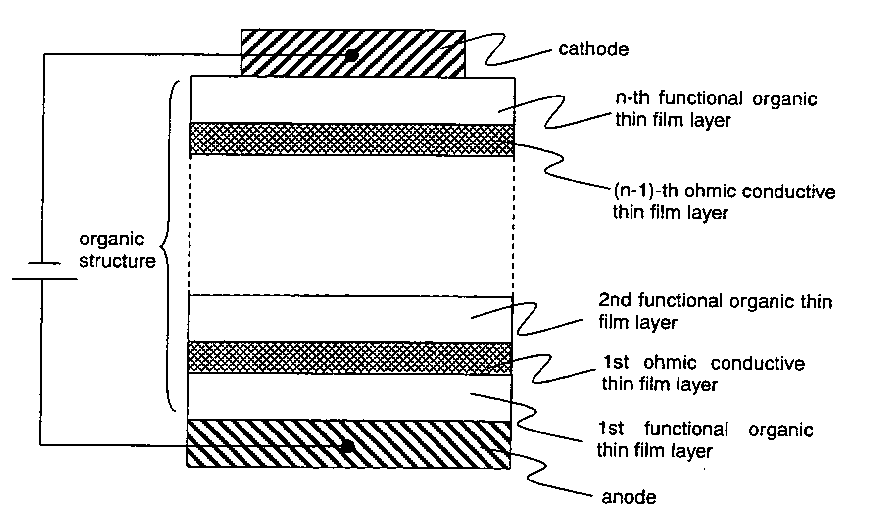
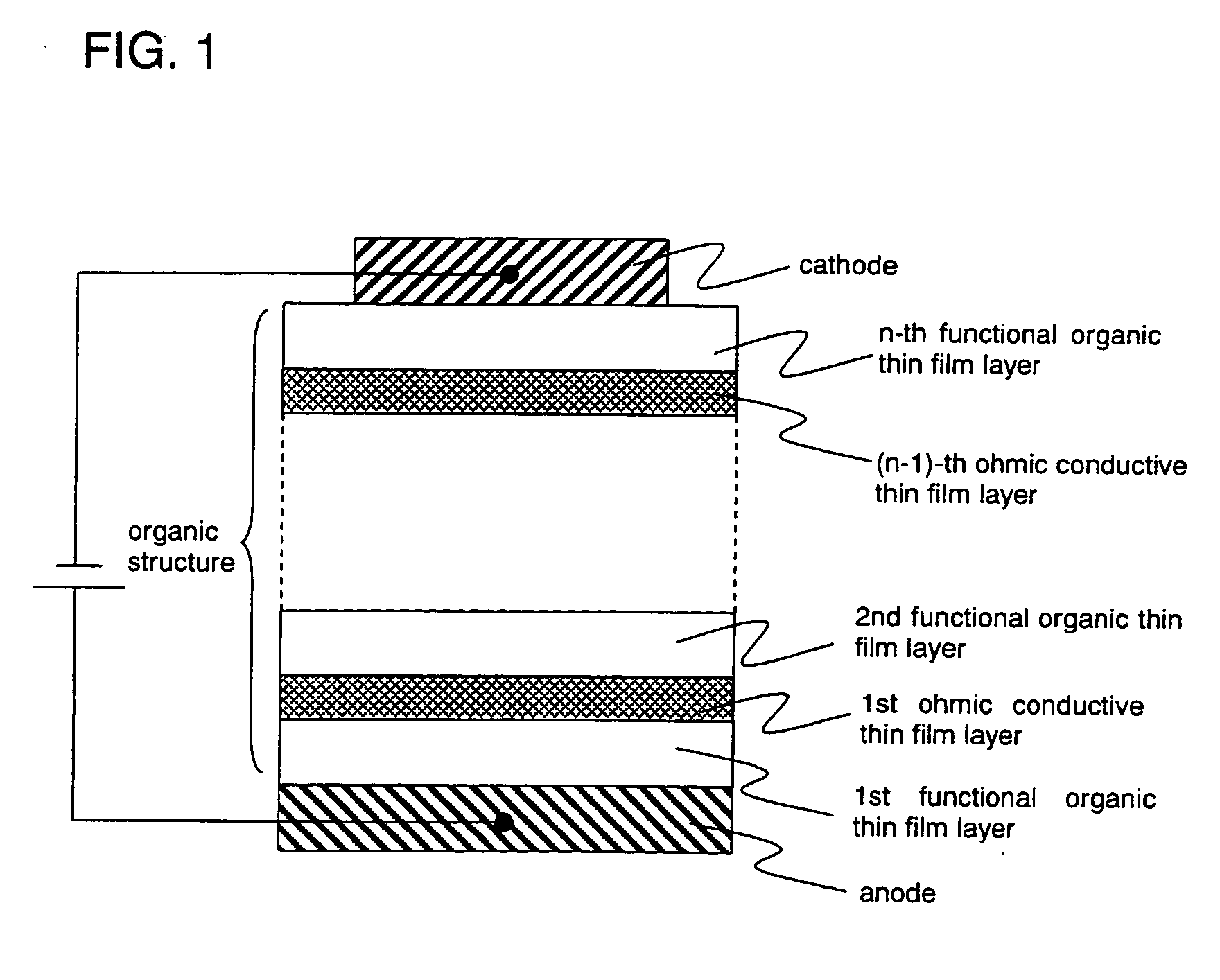
Organic semiconductor element
a technology of organic semiconductor and semiconductor elements, applied in the field of photoelectronic devices, can solve the problems of sclc only being made to flow through a structure, the organic semiconductor itself losing its own physical properties, etc., and achieves the effect of reducing the resistance of sheets and the conductivity ra
- Summary
- Abstract
- Description
- Claims
- Application Information
AI Technical Summary
Benefits of technology
Problems solved by technology
Method used
Image

Examples
embodiments
Embodiment 1
[0129] In accordance with the present embodiment, a specific example will be given of the organic EL element according to the present invention using the charge-transfer complex as the conductive thin film layer. FIG. 8 shows an element structure of the organic EL element.
[0130] First, on a glass substrate 801 on which ITO as an anode 802 is deposited into a film with a thickness of about 100 nm, N—N′-bis(3-methylphenyl)-N,N′-diphenyl-benzidine (abbreviated to TPD) as the hole transporting material is deposited by 50 nm to obtain a hole transporting layer 804a. Next, tris(8-quinolinolato)aluminum (abbreviated to Alq) as a light emitting material having an electron transporting property is deposited by 50 nm to obtain an electron-transporting and light emitting layer 805a.
[0131] A first organic EL layer 810a is formed in the above manner. Thereafter, TTF and TCNQ are codeposited at a ratio of 1:1 as a conductive thin film layer 806, forming a layer with a thickness of ...
embodiment 2
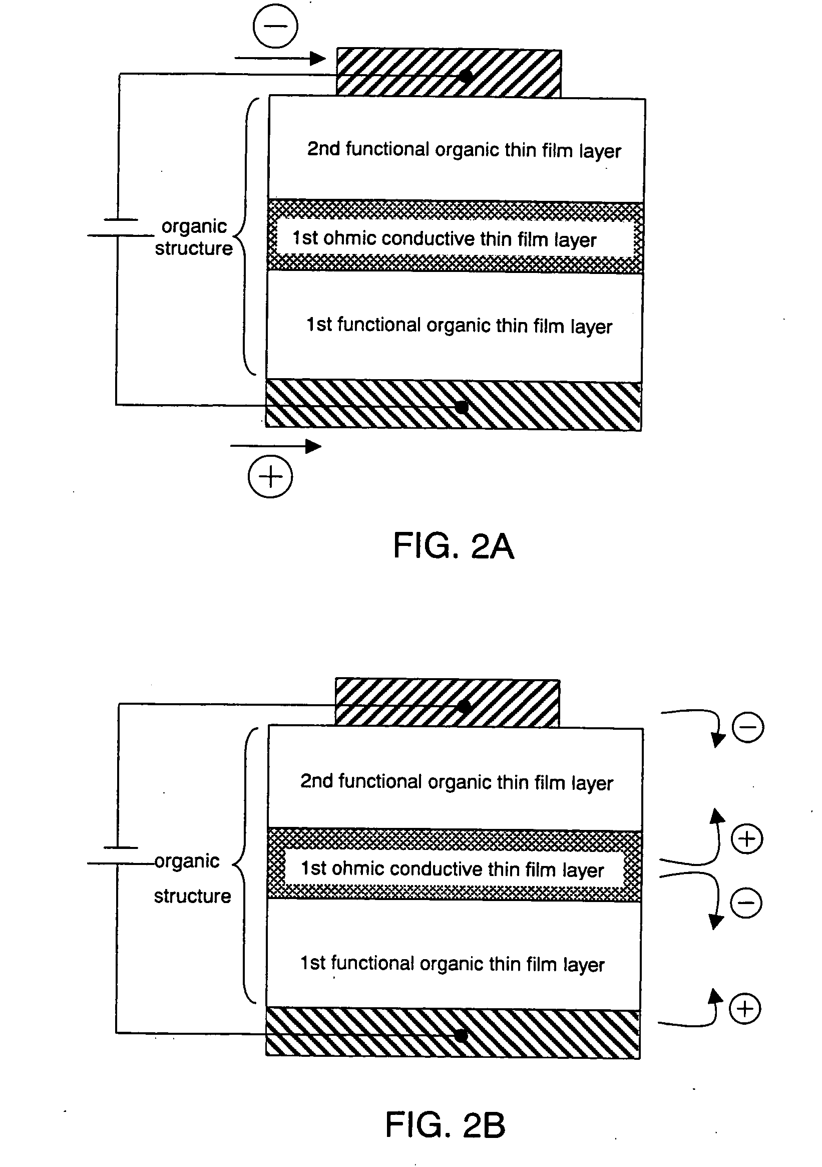
[0134] In accordance with this embodiment, a specific example is shown of an organic EL element of the present invention, in which an organic semiconductor that is the same as used in the organic EL layer is included in the conductive thin film layer, and the acceptor and the donor are doped to make the organic EL element conductive. FIG. 9 shows an example of an element structure of the organic EL element.
[0135] First, 50 nm of TPD for serving as the hole transport material is deposited onto a glass substrate 901 which has approximately 100 nm of ITO serving as an anode 902. Next, 50 nm of Alq which serves as the electron transporting light-emission material is deposited, and this serves as an electron transporting layer / light emitting layer 905a.
[0136] After a first organic EL layer 910a is formed in this way, 5 nm of a layer 906 is codeposited with the Alq so that the donor TTF constitutes 2 mol %. Then, 5 nm of a layer 907 is codeposited with the TPD so that the acceptor TCNQ ...
embodiment 3
[0139] In accordance with the present embodiment, a specific example is shown of a wet-type organic EL element, in which an electrical light emitting polymer is used for the organic EL layer and the conductive thin film layer is formed of a conductive polymer. FIG. 10 shows an element structure of the organic EL element.
[0140] First, onto a glass substrate 1001 on which ITO as an anode 1002 is deposited into a film with a thickness of about 100 nm, a mixed aqueous solution of polyethylene dioxythiophene / polystyrene sulfonic acid (abbreviated to PEDOT / PSS) is applied by spin coating to evaporate moisture, so that a hole injecting layer 1004 is formed with a thickness of 30 nm. Next, poly(2-methoxy-5-(2′-ethyl-hexoxy)-1,4-phenylenevinylene) (abbreviated to MEH-PPV) is deposited into a film with a thickness of 100 nm by spin coating to obtain a light emitting layer 1005a.
[0141] A first organic EL layer 1010a is formed in the above manner. Thereafter, a 30 nm film of PEDOT / PSS is appl...
PUM
 Abstract
Description
Claims
Application Information