Forming nanoscale patterned thin film metal layers

a thin film metal layer and nano-scale technology, applied in the field of nano-scale patterning of metal layers, can solve the problems of complex and expensive systems (established nanolithographic methods, electron beam lithography, deep ultraviolet photolithography, etc., and achieve the effect of high resolution

Inactive Publication Date: 2005-09-20
ALCATEL-LUCENT USA INC +1
View PDF7 Cites 91 Cited by
  • Summary
  • Abstract
  • Description
  • Claims
  • Application Information

AI Technical Summary

Benefits of technology

[0004]This invention is an additive printing method that has high resolution. The method, termed here “nanotransfer printing (nTP)”, involves four components: (i) a stamp (rigid, flexible, or elastomeric) with relief features in the geometry of the desired pattern, (ii) a method for depositing a thin layer of material onto the raised features of this stamp, (iii) a method for bringing the stamp into intimate physical contact with a substrate and (iv) surface chemistries that control adhesion of the deposited material(s) to the stamp relative to the adhesion to the substrate. In some embodiments, the bonding surface chemistry relies o

Problems solved by technology

Established nanolithographic methods (e.g., electron-beam lithography, deep ultraviolet photolithography, etc.) require elaborate and expensive systems that are capable only of patterning a narrow range of specialized materials over small areas on ultraflat surfa

Method used


Image

  • Forming nanoscale patterned thin film metal layers
  • Forming nanoscale patterned thin film metal layers
  • Forming nanoscale patterned thin film metal layers

Examples


Embodiment Construction

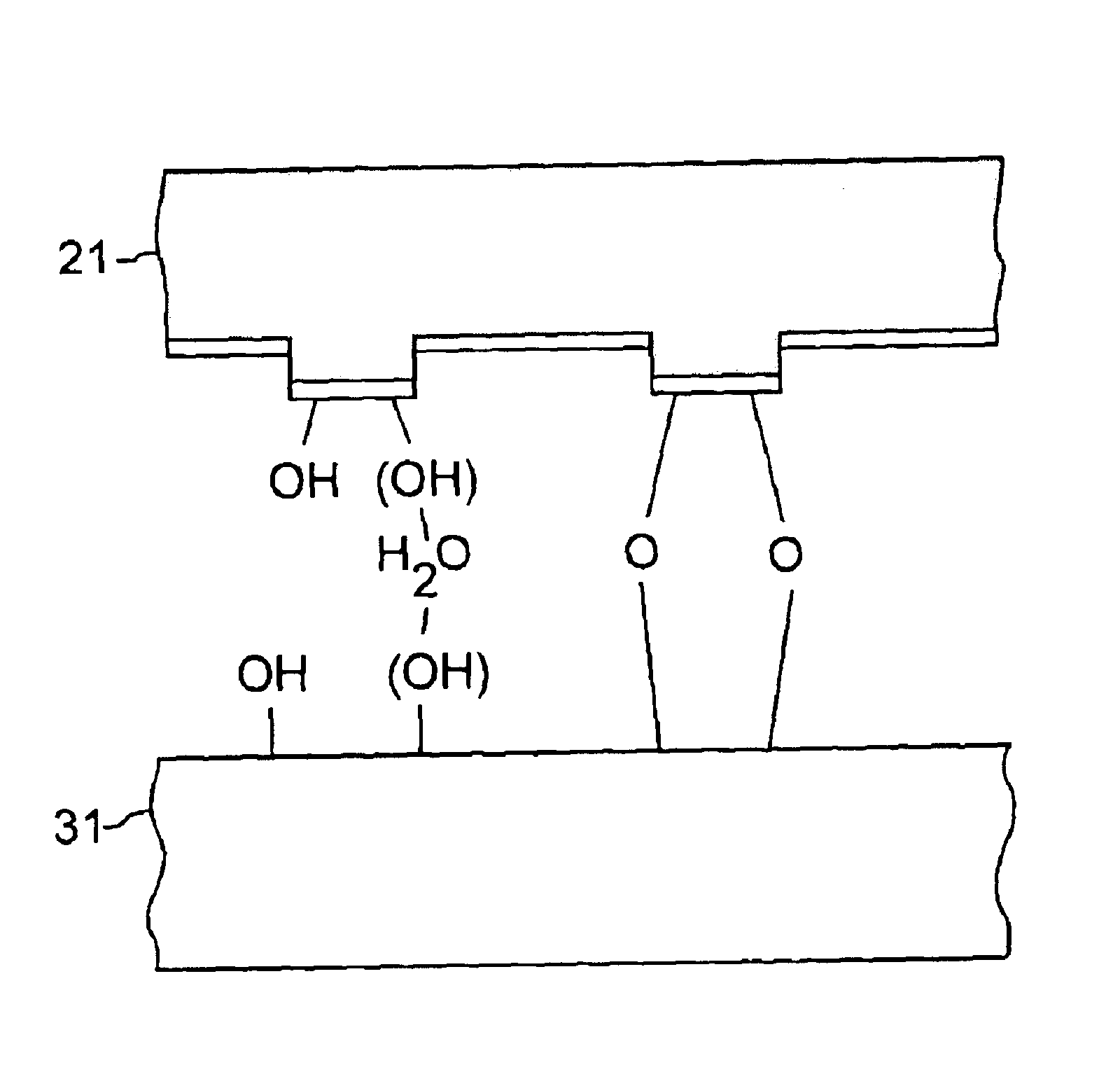
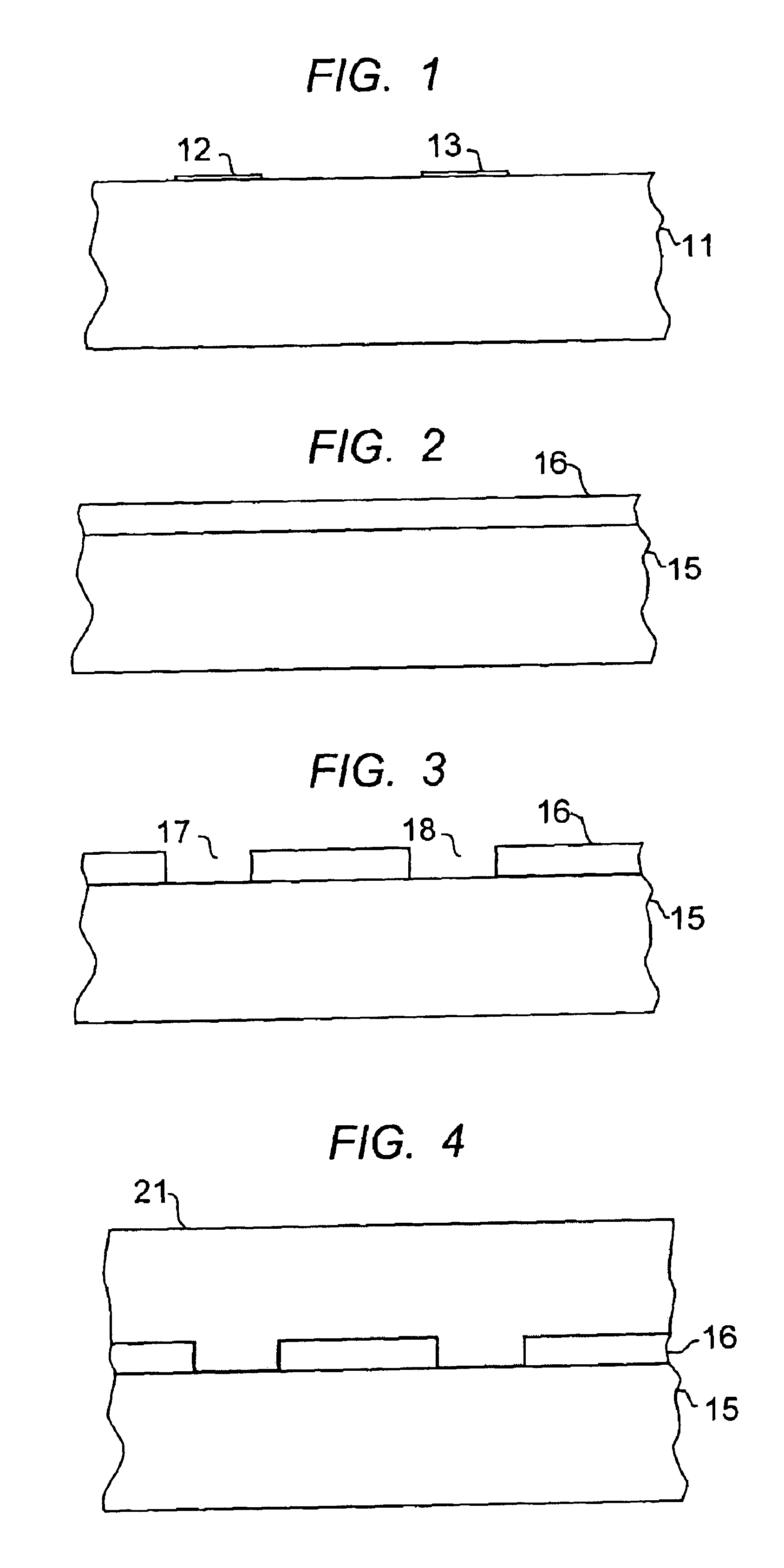
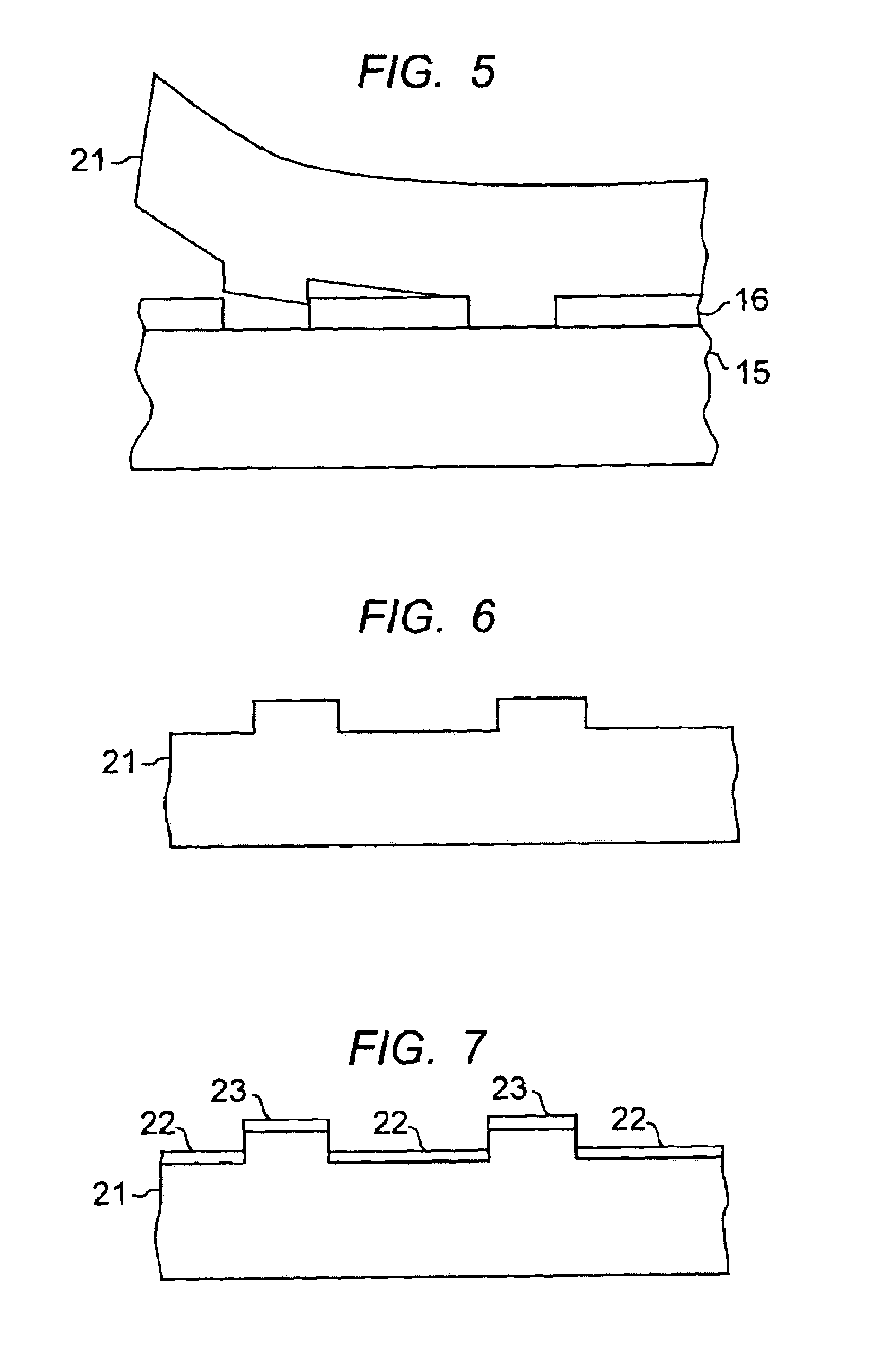
[0013]The method of the invention involves procedures for using nTP with both elastomeric (i.e. conformal) as well as rigid stamps to pattern thin metal films on both conformal and rigid substrates. For purposes of illustration, the method will be described in the context of its application to plastic electronic systems by fabricating drain and source electrodes and appropriate interconnects for high performance n- and p-channel organic transistors and complementary inverter circuits. Typical steps of the nTP method itself will be described with the aid of FIGS. 1-11. FIG. 1 shows the objective of this example. Flexible polymer substrate 11 is shown with source and drain electrodes 12 and 13 formed on the surface of the substrate by nTP. These electrodes are shown by way of example of other TFT features that can be produced by the method of the invention, or other metiallized patterns useful in a wide range of applications as described earlier.

[0014]The nTP method begins with fabric...


PUM


Abstract

The specification describes a contact printing technique for forming patterns of thin films with nanometer resolution over large areas. The procedure, termed here “nanotransfer printing (nTP)”, relies on tailored surface chemistries for transferring thin films, typically metal films, from the raised regions of a stamp to a substrate when these two elements are brought into intimate physical contact. This technique is purely additive, it is fast (<15 s contact times), and the printing occurs in a single processing step at room temperature in open air. nTP is capable of producing patterns with a wide range of features with sizes down to ˜100 nm, and edge resolution better than 25 nm. Electrical contacts and interconnects have been fabricated for high performance organic thin film transistors (TFTs) and complementary inverter circuits, to demonstrate one of the many potential applications for nTP.

Description

FIELD OF THE INVENTION[0001]This invention relates to nanoscale patterning of metal films, and more particularly to patterning of metal films using surface chemistry mediated transfer processes.BACKGROUND OF THE INVENTION[0002](The following section contains background material that, unless specifically stated otherwise, may or may not be prior art).[0003]Advanced techniques for nanofabrication are in widespread use for research in biology, physics, chemistry and materials science. They are also essential manufacturing tools for electronics, photonics and many other existing and emerging areas of technology. Established nanolithographic methods (e.g., electron-beam lithography, deep ultraviolet photolithography, etc.) require elaborate and expensive systems that are capable only of patterning a narrow range of specialized materials over small areas on ultraflat surfaces of rigid inorganic substrates. These limitations and the importance of nanofabrication to progress in nanoscience ...

Claims


Application Information

Patent Timeline
IPC IPC(8): G03F7/00H01L51/40H01L27/12H01L51/05H01L21/00
CPCB82Y10/00B82Y40/00G03F7/0002H01L27/1203H01L51/0001H01L51/0024H01L51/0516H01L51/0004H01L51/0541H01L51/0545H10K71/00H10K71/13H10K71/50H10K10/468H10K10/464H10K10/466
Inventor LOO, YUEH-LINROGERS, JOHN A.
Owner ALCATEL-LUCENT USA INC
Why Eureka
Try Eureka