Electrical connector with hybrid contact set

Active Publication Date: 2020-07-23
FUDING PRECISION COMPONENTS SHENZHEN +1
0 Cites 0 Cited by

AI-Extracted Technical Summary

Problems solved by technology

For the traditional one piece contact, it is relatively hard to get a better balance b...

Benefits of technology

[0004]An object of the invention is to provide an electrical connector with a plurality of contact units each including a first part and a second part mechanically and electrically connected to each other wherein the first part provides the spring contacti...

Abstract

An electrical connector includes a plurality of contact units each having a first part and a second part mechanically and electrically connected to each other wherein the first part provides the spring contacting section for performing the superior mechanical resiliency while the second part provides the mounting section soldered upon the printed circuit board and configured to lower the impedance compared with the first part and provide strong retention thereof.

Application Domain

Technology Topic

Image

  • Electrical connector with hybrid contact set
  • Electrical connector with hybrid contact set
  • Electrical connector with hybrid contact set

Examples

  • Experimental program(1)

Example

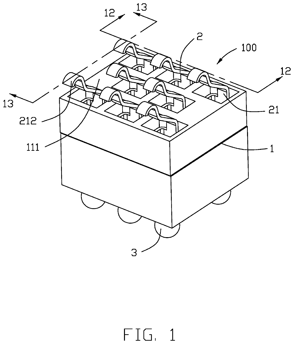
[0019]Referring to FIGS. 1-13, an electrical connector.100 for connecting an electronic package or a CPU (Central Processing Unit) 900 to a printed circuit board 950, includes an insulative housing 1 and a plurality of contacts 2 therein.
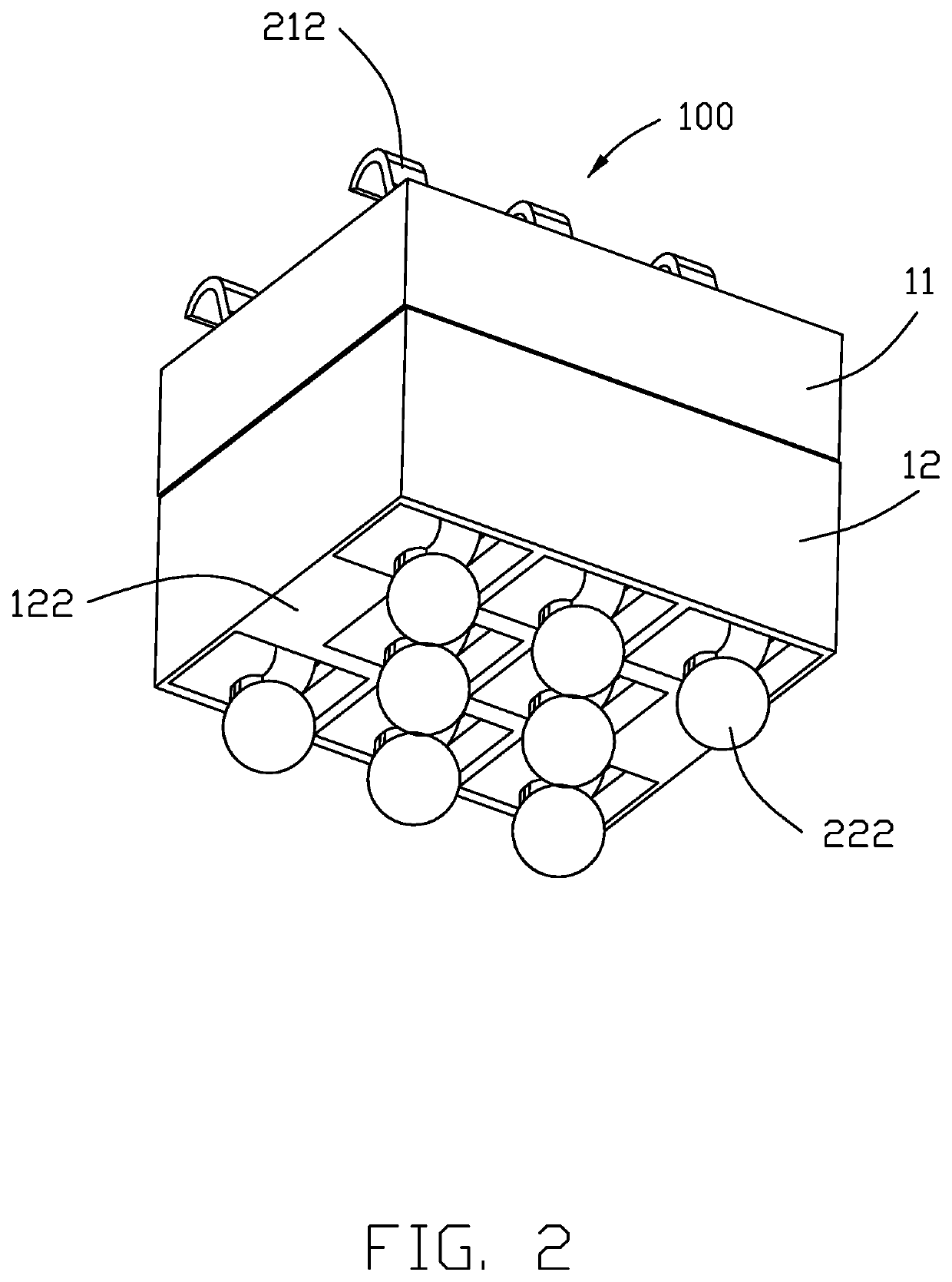
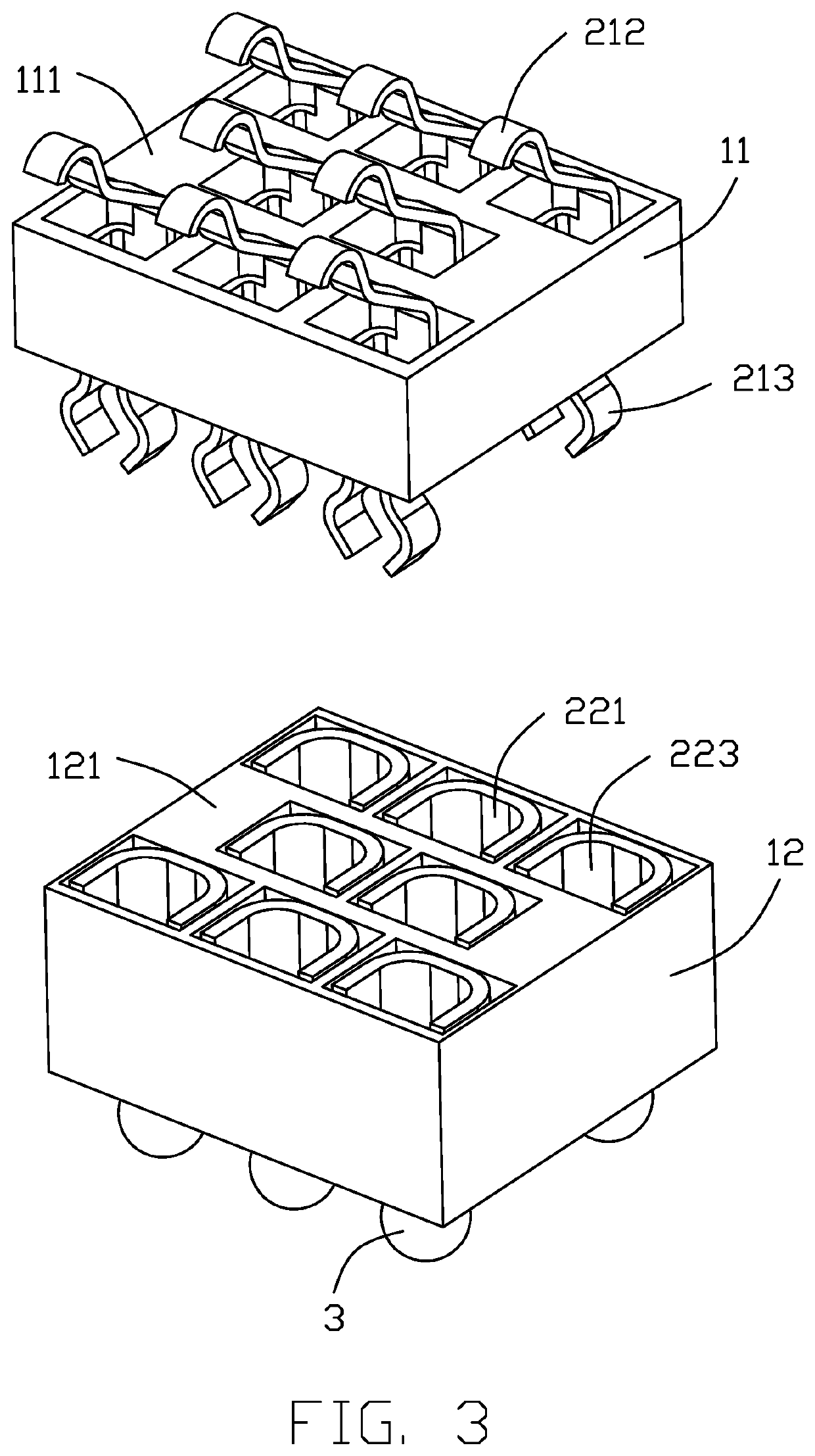
[0020]The housing 1 includes a first/upper insulator 11 having opposite upper surface 111 and lower surface 112, and a second/lower insulator 12 secured upon an upper surface 111 of the first insulator 11 and having opposite upper surface 121 and the lower surface 122. The first insulator 11 includes a plurality of first/upper passageways each having a first receiving slot 113 and a securing slot 114 adjacent thereto. The second insulator 12 includes a plurality of second/lower passage or receiving slots 23 in alignment with the corresponding first receiving slots 113, respectively, in the vertical direction.
[0021]The contact includes a first/upper part 21 and a second/lower part 22. The first part 21 is retained to the first insulator 11 while the second part 22 is retained to the second insulator 12 and constantly mechanically and electrically connected to the first part 21. Preferably, the first part 21 and the second part 22 are soldered with each other. The first part 21 includes a first body 211 secured to the first insulator 11, and a contacting section 212 extending upwardly from the first body 211 and above the upper surface 111 of the first insulator 11. The second part 22 includes a second body 221 and a soldering leg 222 extending downwardly from the second body 221 and beyond/below the lower surface 122 of the second insulator 12. The first part 21 further includes a first/upper linking section 213 and the second part 22 further includes a second/lower linking section 223 mechanically and electrically connected to the first linking section 213. Preferably, the first linking section 213 is soldered to the second linking section 223.
[0022]The first body 211 forms a U-shaped structure, and the first linking section 213 includes a pair of spring tangs linked to the first body 211 via the first connecting sections 214 of the first body 211 and configured with convex sections 2131 and the concave sections 2132 wherein the first linking section 213 is linked to the second linking section 223 via the convex sections 2131. The second linking section 223 forms a U-shaped structure, and the pair of spring tangs of the first linking section 213 is inserted within and contact the second linking section 223. The first linking section 213 is partially located in the first receiving slot 113 and partially extends below the lower surface 112 of the first insulator 11, while the first body 211 is retained in the securing slot 114. The second body 221 of the second part 22 is received within the second receiving slot 123. The second part 22 further includes a connecting section 225 linked between the second body 221 and the leg 222.
[0023]The second linking section 223 forms a barbed structure 224 to retain the second part 22 in the corresponding second receiving slot 123 in the second insulator 12. The first linking section 213 extends into the second receiving slot 123 to contact the second linking section 223. Optimally, solder attachment may be applied to an interface between the first linking section 213 and the second linking section 223.
[0024]In this embodiment, both first part 21 and the second part 22 are derived from sheet metal via stamping and forming wherein a thickness of the first part 21 is smaller than that of the second part 22. For example, the first part 21 may adopt a thickness of 0.05 mm˜0.08 mm while the second part 22 may adopt a thickness of 0.2 mm˜0.4 mm with the superior conductivity thereof. Understandably, the relative thicker second part 22 not only reliably retains the contact 2 with regarding to the insulative housing 1 but also provides a preferred impedance thereof, and the relatively thin first part 21 may provide the desired resiliency for lowering the improper normal force between the CPU 900 and the contact 2.
[0025]While a preferred embodiment in accordance with the present disclosure has been shown and described, equivalent modifications and changes known to persons skilled in the art according to the spirit of the present disclosure are considered within the scope of the present disclosure as described in the appended claims.

PUM

no PUM

Description & Claims & Application Information

We can also present the details of the Description, Claims and Application information to help users get a comprehensive understanding of the technical details of the patent, such as background art, summary of invention, brief description of drawings, description of embodiments, and other original content. On the other hand, users can also determine the specific scope of protection of the technology through the list of claims; as well as understand the changes in the life cycle of the technology with the presentation of the patent timeline. Login to view more.

Similar technology patents

Display panel and display module

Owner:WUHAN CHINA STAR OPTOELECTRONICS TECH CO LTD

Classification and recommendation of technical efficacy words

  • Strong retention
  • Lower impedance

Multi-unmanned-aerial-vehicle communication relay platform collaborative autonomous layout method

ActiveCN108718454AStrong retentionFast and efficient deploymentRadio transmissionNetwork planningTerrainReal-time computing
Owner:中国人民解放军火箭军工程大学

Complete denture and preparation method thereof

ActiveCN107981944AStrong retentionIncrease retentionArtificial teethAlveolar crestDentures
Owner:SHANDONG UNIV

Water-absorption-type temperature lowering particles and preparation method thereof

InactiveCN105218749AStrong retentionImprove thermal conductivityMaterials sciencePolyacrylic acid
Owner:CIXI LINGDONG ELECTRONICS TECH
Why Eureka
Try Eureka