Passive photoelectric tag

Inactive Publication Date: 2020-08-06
ZTE CORP
4 Cites 0 Cited by

AI-Extracted Technical Summary

Problems solved by technology

Therefore, the common passive RFID tag has large electromagnetic radiation, and long-term use of the common passive RFID tag is harmful to the human body.
In addition, considering effects of the electroma...

Method used

[0042]The passive photoelectric tag realizes power provision and signal receiving through a photocell, and power supply is not needed, the cost and the size of the passive photoelectric tag is reduced and the service life of the passive photoelectric tag is prolonged.
[0044]By using the photocell to receive a visible light signal, effective reception and detection of a signal can be achieved by a light reception and detection capability of the photocell, and moreover the photocell can provide a power supply voltage for working of a photoelectric tag through conversion from optical energy to electrical energy, so as to form a non-contact novel passive photoelectric tag. Compared with existing photoelectric tags, the novel passive photoelectric tag is low in cost, small in size, and has a longer service life, and overcomes a disadvantage that the passive radio frequency tag is large in electromagnetic radiation and harmful to a human body.
[0059]In an implementation manner of the embodiments of the disclosure, the power management module 1031 includes a voltage regulator, the voltage regulator includes a band-gap reference, a start-up circuit, an error amplifier, and serves to process a received DC signal to obtain a stable voltage source and provides a power supply voltage to other modules. Power management, having good stability, high power supply rejection (PSR), good linear adjustment rate and load regulation rate, and a low temperature coefficient, can ensure stable working of the receiver. Since a passive structure is adopted, power consumption should be reduced in the meantime of meeting basic performance indices.
[0061]The digital circuit module 1033 mainly includes a decoder unit, a digital baseband, a memory, and an encoder unit, and mainly serves to perform encoding and decoding processing and data control to the digital signal extracted from the receiver module and generates a signal to be transmitted back to a reader-writer. A digital circuit module based on a reasonable communication protocol may have a stronger anti-interference performance and a lower error rate.
[0063]The LED driving circuit module 1035 adopts a signal transmitted back to the reader-writer from the digital circuit module to drive the LED emission unit 104 so as to realize normal working of the LED emission unit 104. Since the LED driving circuit module accounts for the largest proportion of overall power consumption, realization of low power consumption of the LED driving circuit module is the key to achieve overall low power consumption of a tag.
[0066]In the embodiment of the...

Benefits of technology

[0030]The passive photoelectric tag provided according to the embodiments of the disclosure includes: a photocell, which is used to receive an optical signal; a service separation unit, which is used to separate the optical signal received by the photocell into a DC voltage and an AC signal; a transceiver unit, which is used to perform photoelectric conversion processing and electric signal processing on an optical signal in the AC signal under...

Abstract

The disclosure relates to the technology of optical communication, and specifically, to a passive photoelectric tag. The passive photoelectric tag includes: an photocell used to receive an optical signal; a service separation unit used to separate the received optical signal into a DC voltage and an AC signal; a transceiver unit used to perform photoelectric conversion and electric signal processing on an optical signal in the AC signal under power supply of the DC voltage to generate a signal to be transmitted; and an LED emission unit used to transmit the signal to be transmitted in a form of an optical signal. The passive photoelectric tag realizes power provision and signal receiving through a photocell, and power supply is not needed, the cost and the size of the passive photoelectric tag is reduced and the service life of the passive photoelectric tag is prolonged.

Application Domain

Record carriers used with machinesSensing by electromagnetic radiation

Technology Topic

TransceiverOptical communication +8

Image

  • Passive photoelectric tag
  • Passive photoelectric tag

Examples

  • Experimental program(1)

Example

[0036]The technical solutions in embodiments of the disclosure will be explained clearly and completely with reference to the accompanying drawings in the embodiments of the disclosure. Obviously, the embodiments described are only some embodiments of the disclosure, rather than all of the embodiments of the disclosure. All other embodiments obtained by those skilled in the art based on the embodiments of the disclosure under the premise that no creative work is involved fall within the protection scope of the disclosure.
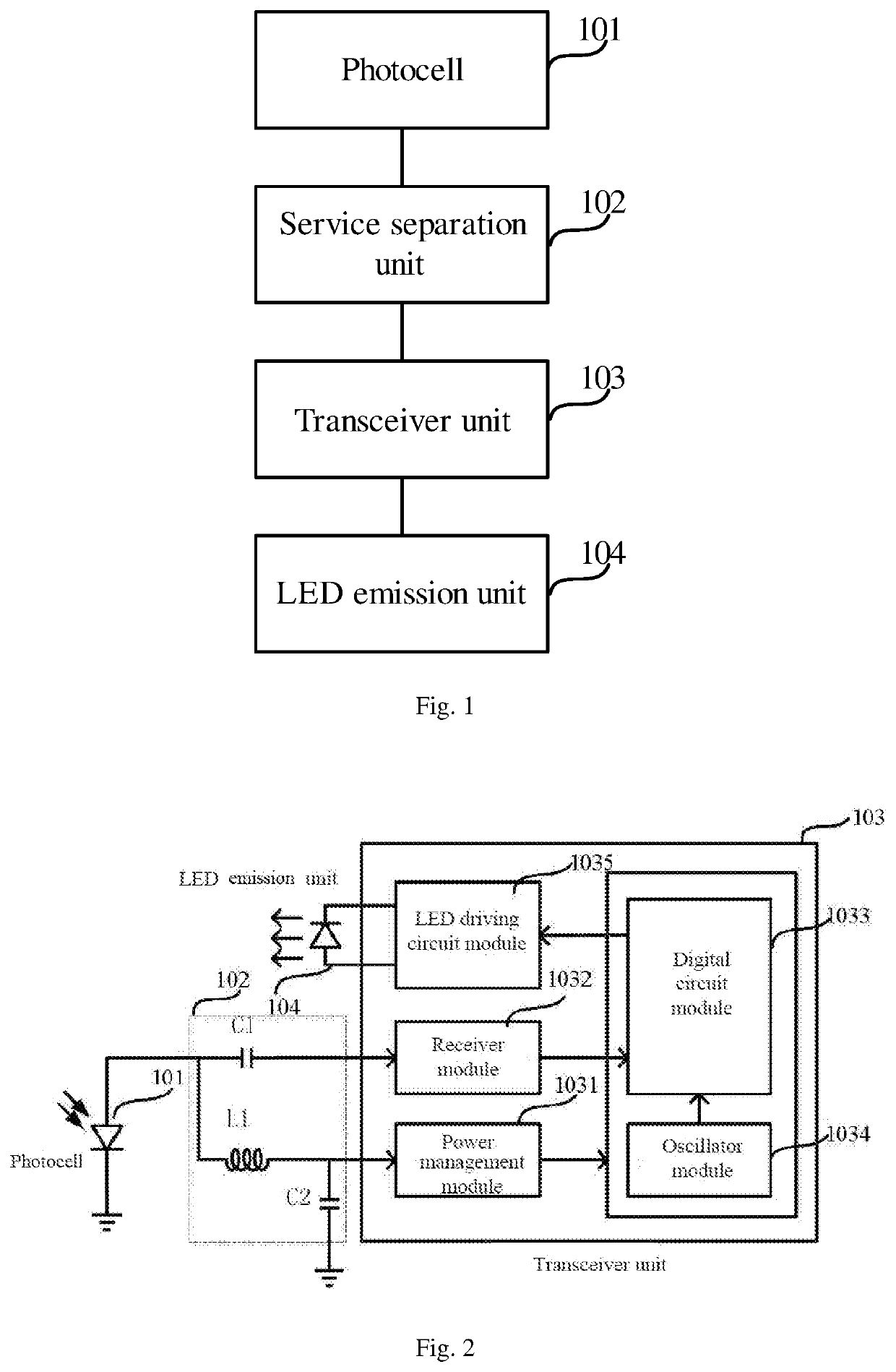
[0037]As shown in FIG. 1, a passive photoelectric tag provided by the embodiments of the disclosure includes:
[0038]a photocell 101, configured to receive an optical signal;
[0039]a service separation unit 102, connected with the photocell 101, and configured to separate the optical signal received by the photocell 101 into a DC voltage and an AC signal;
[0040]a transceiver unit 103, connected with the service separation unit 102, and configured to perform photoelectric conversion processing and electric signal processing on an optical signal in the AC signal under power supply of the DC voltage to generate a signal to be transmitted; and
[0041]an LED emission unit 104, connected with the transceiver unit 103, and configured to transmit the signal to be transmitted in a form of an optical signal.
[0042]The passive photoelectric tag realizes power provision and signal receiving through a photocell, and power supply is not needed, the cost and the size of the passive photoelectric tag is reduced and the service life of the passive photoelectric tag is prolonged.
[0043]An internal working manner of the passive photoelectric tag is as follows: the photocell 101 separates a received external visible light signal into two parts through the service separation unit 102. One part of the light is converted into electric energy required for working of the tag, and the converted electric energy provides energy for each unit; the other part of the light signal carrying a signal undergoes a photoelectric conversion processing through the transceiver unit 103, and after the processed electric signal undergoes a electric signal processing, a signal is loaded and transmitted through the LED emission unit 104.
[0044]By using the photocell to receive a visible light signal, effective reception and detection of a signal can be achieved by a light reception and detection capability of the photocell, and moreover the photocell can provide a power supply voltage for working of a photoelectric tag through conversion from optical energy to electrical energy, so as to form a non-contact novel passive photoelectric tag. Compared with existing photoelectric tags, the novel passive photoelectric tag is low in cost, small in size, and has a longer service life, and overcomes a disadvantage that the passive radio frequency tag is large in electromagnetic radiation and harmful to a human body.
[0045]In the embodiments of the disclosure, the photocell is adopted to replace a common photodiode to serve as a visible light detector. After being irradiated by an LED visible light signal, the photocell generates a constantly changing DC voltage which can be regarded as a superposition of a constant DC voltage and an AC voltage. The constant DC voltage can provide a power supply voltage required by a receiver through circuit processing, so as to obtain a novel passive photoelectric tag.
[0046]In practical disclosure, the photocell may include a solar cell. For example, a gallium arsenide solar cell of 10 mm×10 mm×2 mm or a monocrystalline silicon solar cell of 30 mm×30 mm×5 mm may be used.
[0047]In an implementation manner of the embodiments of the disclosure, as shown in FIG. 2, the service separation unit 102 specifically includes:
[0048]a first capacitor C1 used to isolate a DC signal and extract an AC signal, and a low-pass filter connected in parallel with the first capacitor C1 and used to extract a DC voltage.
[0049]In an implementation manner of the embodiments of the disclosure, the low-pass filter includes: an inductor L1 and a second capacitor C2, in which
[0050]an end of the inductor L1 is connected with the photocell 101, and another end thereof is connected with the second capacitor C2 and the transceiver unit 103, another end of the second capacitor C2 is grounded.
[0051]Specifically, the service separation unit 102 includes two branches. One branch is the first capacitor C1 which may isolate a DC signal and extract and send an AC signal to the transceiver 103 for processing. The other branch includes the low-pass filter formed by an LC. In the low-pass filter, a voltage at two ends of the second capacitor C2 is a DC voltage. The AC signal with a high frequency is blocked by the inductor L1, and has little effect on the voltage at two ends of the second capacitor C2. At last, the voltage at two ends of the second capacitor C2 is input into the transceiver unit 103 to provide power supply to the transceiver unit 103.
[0052]A chip capacitor having the largest capacitance value can be used as the second capacitor C2.
[0053]In an implementation manner of the embodiments of the disclosure, as shown in FIG. 2, the transceiver unit 103 specifically includes:
[0054]a power management module 1031, connected with an output end of a DC voltage of the service separation unit 102, and configured to process the DC signal to obtain a stable voltage source and to provide a power supply voltage for other modules;
[0055]a receiver module 1032, connected with an output end of an AC signal of the service separation unit 102, and configured to process the AC signal to obtain a digital signal;
[0056]a digital circuit module 1033, connected with the receiver module 1032, and configured to perform encoding and decoding processing and data control to the digital signal to generate a signal to be transmitted;
[0057]an oscillator module 1034, connected with the digital circuit module 1033, and configured to generate a clock oscillation signal; and
[0058]an LED driving circuit module 1035, connected with the digital circuit module 1033, and configured to convert the signal to be transmitted into an optical signal and to drive the LED emission unit 104 to transmit the optical signal.
[0059]In an implementation manner of the embodiments of the disclosure, the power management module 1031 includes a voltage regulator, the voltage regulator includes a band-gap reference, a start-up circuit, an error amplifier, and serves to process a received DC signal to obtain a stable voltage source and provides a power supply voltage to other modules. Power management, having good stability, high power supply rejection (PSR), good linear adjustment rate and load regulation rate, and a low temperature coefficient, can ensure stable working of the receiver. Since a passive structure is adopted, power consumption should be reduced in the meantime of meeting basic performance indices.
[0060]The receiver module 1032 mainly includes an equalization circuit, a limiting amplifier circuit, and a comparator circuit, and serves to perform limiting amplification to an input AC digital, and then a signal is processed by a comparator, a digital signal is extracted for a further process through a digital circuit. In the design, realization of low power consumption in a circuit should also be paid attention to.
[0061]The digital circuit module 1033 mainly includes a decoder unit, a digital baseband, a memory, and an encoder unit, and mainly serves to perform encoding and decoding processing and data control to the digital signal extracted from the receiver module and generates a signal to be transmitted back to a reader-writer. A digital circuit module based on a reasonable communication protocol may have a stronger anti-interference performance and a lower error rate.
[0062]The oscillator module 1034 serves to generate a clock oscillation signal for use in working of a digital circuit, and may use a ring oscillation structure or a relaxation oscillation structure. Stability of an oscillation frequency is a main parameter of the oscillator module. Oscillation frequency of a good oscillator is less affected by voltage, temperature, and the process, which can ensure precision of working of the digital circuit.
[0063]The LED driving circuit module 1035 adopts a signal transmitted back to the reader-writer from the digital circuit module to drive the LED emission unit 104 so as to realize normal working of the LED emission unit 104. Since the LED driving circuit module accounts for the largest proportion of overall power consumption, realization of low power consumption of the LED driving circuit module is the key to achieve overall low power consumption of a tag.
[0064]The LED emission unit 104 transmits a signal back to the reader-writer in the form of an optical signal to complete optical signal communication. In order to put an LED into a driving circuit for simulation, the LED needs to be modeled, and a spice model or a veriloga model of the LED is put into a circuit for simulation.
[0065]As a preferred embodiment, an external solar cell may be used as a photocell. The solar cell may effectively absorb visible light, and convert an optical signal into an electric signal so as to generate a changing DC voltage. A DC signal and an AC signal are separated via a passive circuit network of a service separation unit, and are respectively provided to a power management module and a receiver module, so as to achieve a function of receiving optical signals. The solar cell can be made of materials such as monocrystalline silicon, polycrystalline silicon, gallium arsenide, and so on. Considering the size, the cost, and efficiency of optical energy conversion comprehensively, and under the premise that the solar cell stably provides power supply to a receiver, a solar cell satisfying requirements may be selected eclectically, such as a gallium arsenide solar cell of 10 mm×10 mm×2 mm, a monocrystalline silicon solar cell of 30 mm×30 mm×5 mm, and the like. It should be specifically pointed out that the size of the solar cell accounts for the largest proportion of the size of an overall passive photoelectric tag and limits the size of a tag. Moreover, the size of the photocell and efficiency of optical energy conversion also limit the amount of energy that the photocell supplies to an internal circuit of the tag, and also affect a working distance of the overall photoelectric tag. Therefore, those skilled in the art can take multiple factors into account when selecting a photocell.
[0066]In the embodiment of the disclosure, as shown in FIG. 2, a service separation unit 102 serves to separate a changing voltage generated by the solar cell into a DC signal and an AC signal. Specific implementation is as follows: according to a data transmission rate required by visible light communication, a proper capacitor C1 is selected, so that an AC voltage signal may enter the receiver with little attenuation. L1 and C2 form a low-pass filter which serves to extract a DC voltage signal to supply a power management module. A larger value may be selected for an inductor L1 which has very large impedance when the frequency is higher, so that AC signals are blocked from two ends of the C2. A chip capacitor with a value larger than a set value may be selected for a capacitor C2. On one hand, effects of an AC signal can be reduced; and on the other hand, a large amount of charge can be stored, and it is ensured that a stable voltage may still be provided when a visible light signal changes due to sudden interference.
[0067]As shown in FIG. 2, the receiver module 1032 may adopt an optical receiver structure in traditional visible light communication so as to extract a digital signal from a weak electric signal to input the digital signal into a digital circuit module.
[0068]As shown in FIG. 2, a power management module 1031, a digital circuit module 1033, and an oscillator module 1034 may be designed according to circuit structures of corresponding modules in a traditional RFID passive tag so as to realize functions of corresponding modules.
[0069]As shown in FIG. 2, LED driving circuit module 1035 may adopt a simple series structure, and an LED may be driven by a signal that is transmitted by the digital circuit module back to a reader-writer. As a preferred example, since the LED itself has a larger junction capacitance, an LED electricity release loop may be added to an LED driving circuit so as to increase a working bandwidth of the circuit. In addition, considering that leakage interference should be minimized, as shown in FIG. 1, the distance between a wavelength of an LED and a LED wavelength of a visible light of the reader-writer should be long enough to achieve wavelength division isolation. As a preferred example, a visible light may be selected for the LED of the reader-writer to transmit, and a light with different wavelength from a wavelength of the LED of the reader-writer may be selected for an LED in a photoelectric tag to transmit.
[0070]In an implementation manner of the embodiments of the disclosure, a distance between a wavelength of the LED emission unit and an LED wavelength of a visible light of the reader-writer may be larger than a set value. The LED emission unit can use a visible light with a different wavelength from a wavelength of the LED of the reader-writer to transmit.
[0071]A structure of the digital circuit module 1033 is schematically shown in FIG. 3, and the digital circuit module 1033 mainly includes an encoder, a decoder, a digital baseband circuit, and a memory. A digital signal extracted from the receiver enters the decoder for decoding. A decoded signal is processed by the digital baseband circuit, and carrying out data communication with the memory. In this way, a digital signal that needs to be transmitted back to the reader-writer is obtained. The digital signal that needs to be transmitted back is encoded by the encoder, and an obtained signal is converted by the LED driving circuit into an optical signal which is transmitted back to the reader-writer.
[0072]Besides, optical communication between a passive photoelectric tag and a reader-writer is shown in FIG. 4. After an LED of the reader-writer emits visible light carrying information, a photocell in the tag, on one hand, is being charged and converts an optical signal carrying information into an electric signal on the other hand. When charging energy meets requirements for power consumption of an internal circuit of the tag, the circuit works normally. A digital signal is extracted and processed, and returned data is converted into an optical signal carrying information via an LED and a driving circuit thereof. The returned optical signal is received by a photoelectric detector (PD) of the reader-writer for further processing. As can be seen, if a peak value of an LED emission spectrum in the passive photoelectric tag and a peak value of reception spectrum sensitivity of the PD in the reader-writer correspond to a same wavelength range, it means that energy utilization rate is improved, which is beneficial for reducing power consumption of an LED driving circuit. Overall power consumption of the photoelectric tag may be reduced accordingly.
[0073]By using a photocell to receive a visible light signal, the light reception and detection capability of the photocell realizes effective signal reception and detection, and moreover the photocell can provide a power supply voltage for working of a photoelectric tag through conversion from optical energy to electrical energy, so as to form a non-contact novel passive photoelectric tag. Compared with existing photoelectric tags, the novel passive photoelectric tag is low in cost, small in size, and has a longer service life, and overcomes a disadvantage that the passive radio frequency tag is large in electromagnetic radiation and is harmful to a human body.
[0074]Various embodiments in the description are described in a progressive manner, and reference can be made to other embodiments for the same or similar parts between various embodiments, and the description of each embodiment focuses on its difference from other embodiments. In particular, the description of a device embodiment is relatively simple since the device embodiment is basically similar to a method embodiment, and reference can be made to related description of the method embodiment.
[0075]Although the disclosure is described by way of embodiments, it is known to those skilled in art that many variations and modifications can be made to the disclosure without departing from the spirit and scope of the disclosure. Therefore, if these modifications and variations fall within the scope of claims of the disclosure and equivalent technologies thereof, it is intended that these modifications and variations are also covered in the disclosure.
INDUSTRIAL APPLICABILITY
[0076]The passive photoelectric tag provided according to the embodiments of the disclosure includes: a photocell used to receive an optical signal; a service separation unit used to separate the optical signal received by the photocell into a DC voltage and an AC signal; a transceiver unit used to perform photoelectric conversion processing and electric signal processing on an optical signal in the AC signal under power supply of the DC voltage to generate a signal to be transmitted; and an LED emission unit used to transmit the signal to be transmitted in a form of an optical signal,. The passive photoelectric tag realizes power provision and signal receiving through a photocell, and power supply is not needed, the cost and the size of the passive photoelectric tag is reduced and the service life of the passive photoelectric tag is prolonged.

PUM

no PUM

Description & Claims & Application Information

We can also present the details of the Description, Claims and Application information to help users get a comprehensive understanding of the technical details of the patent, such as background art, summary of invention, brief description of drawings, description of embodiments, and other original content. On the other hand, users can also determine the specific scope of protection of the technology through the list of claims; as well as understand the changes in the life cycle of the technology with the presentation of the patent timeline. Login to view more.

Similar technology patents

Process for purification of a synthesis gas containing hydrogen and impurities

ActiveUS20160146535A1reduction of it valuereduction in size and cost
Owner:CASALE SA

Sheet bundle binding device and image forming system having the same

InactiveUS20170087795A1reduction in size and cost
Owner:COPYER

Transmission

ActiveUS20140076080A1reduction in size and costpassenger comfort in be enhance
Owner:SUBARU CORP

Motion and control system

InactiveUS20150207440A1reduction in size and cost
Owner:SCHNEIDER TOSHIBA INVERTER EUROPE SAS

Classification and recommendation of technical efficacy words

  • reduction in size and cost
  • prolong service life

System and Method for Regulation of Solid State Lighting

ActiveUS20090079359A1reduction in size and costlong battery life
Owner:CHEMTRON RES

Motor controller

ActiveUS20060108957A1reduce powerreduction in size and cost
Owner:MITSUBISHI ELECTRIC CORP

Pwm drive apparatus and method for correcting output offset thereof

InactiveUS20080130186A1reduction in size and costreduce output offset
Owner:COLLABO INNOVATIONS INC

Inspecting apparatus, and inspecting method

InactiveUS20100165094A1reduction in size and costreadily detect
Owner:I-PULSE CO LTD

Parallel-connected LED illuminant and LED light lamp

ActiveUS20170167667A1enlarge effective heat dissipation areaprolong service life
Owner:SHANDONG PROSPEROUS STAR OPTOELECTRONICS TECH CO LTD

Combination of outer motor and control box therefor

ActiveUS20120104907A1simple and cost effective production processprolong service life
Owner:ZHONGSHAN BROAD OCEAN
Why Eureka
Try Eureka