Semi-conductor wafers longer than industry standard square

a technology of semi-conductor and square, which is applied in the direction of conveyor parts, final product manufacturing, transportation and packaging, etc., can solve the problems of very small cost of additional silicon, and achieve the effects of small cost, small amount of additional surface area, and fast processing speed

Active Publication Date: 2020-08-06
CUBICPV INC
View PDF18 Cites 0 Cited by
  • Summary
  • Abstract
  • Description
  • Claims
  • Application Information

AI Technical Summary

Benefits of technology

[0019]The instant application reports that wafers can be made according to a relatively new process, known as the Direct Wafer (DW) making process, described in the below referenced DW patents, and that such wafers can be made that have the industry standard size A (presently 156 mm+ / −1 mm) as the dimension of one side, referred to herein as its width, and a longer perpendicular dimension, referred to herein as its length. This added length, compared to a square wafer of dimensions A×A, provides a very large amount of additional surface area. The wafers with industry-standard width and greater than industry-standard length disclosed herein can be processed in the vast majority of currently used wafer processing and handling equipment, either without any modification to the equipment, or, with modifications that are relatively simple, conceptually, and modest in cost, as compared to the cost savings that arise from the additional surface area of use. A further advantage of wafer and module manufacturing cost and economies is that the cost of handling a slightly larger wafer is almost zero. The cost of the additional silicon is very small, and, in any case, that silicon would have been part of the cost of a different wafer. Thus, it is not actually an additional cost of the entire solar collecting apparatus. Thus, the economies of handling the much larger amount of surface area for the same number of pieces of (slightly larger) silicon wafers are such that it is well worth the effort.

Problems solved by technology

The cost of the additional silicon is very small, and, in any case, that silicon would have been part of the cost of a different wafer.

Method used


Image

  • Semi-conductor wafers longer than industry standard square
  • Semi-conductor wafers longer than industry standard square
  • Semi-conductor wafers longer than industry standard square

Examples


Embodiment Construction

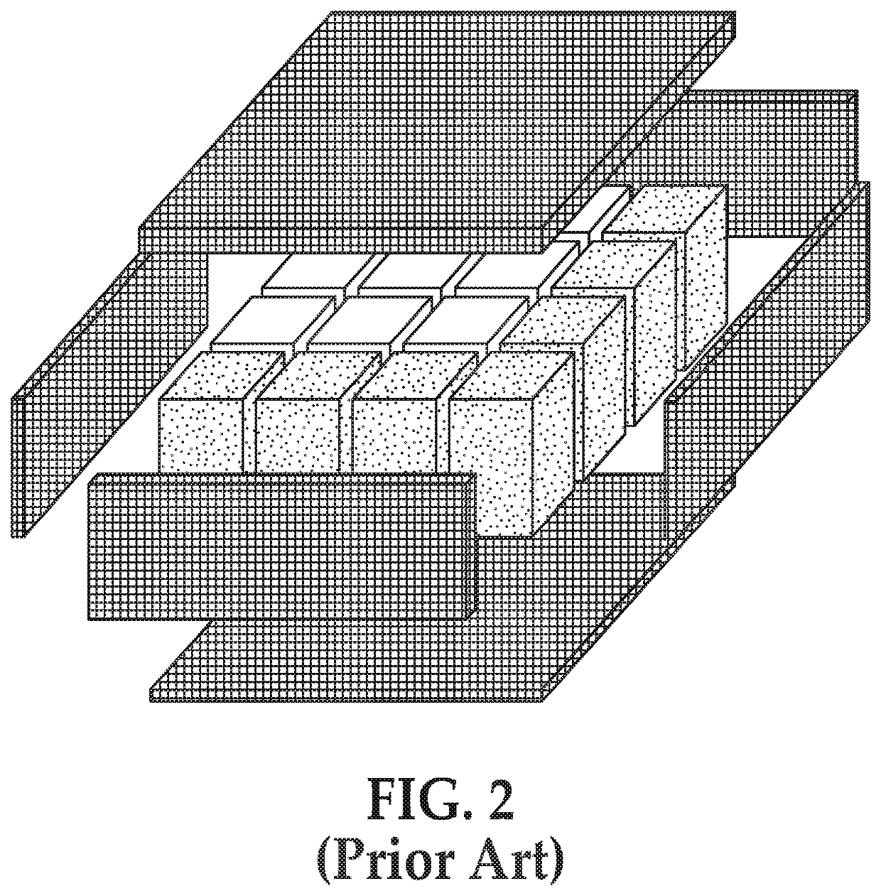
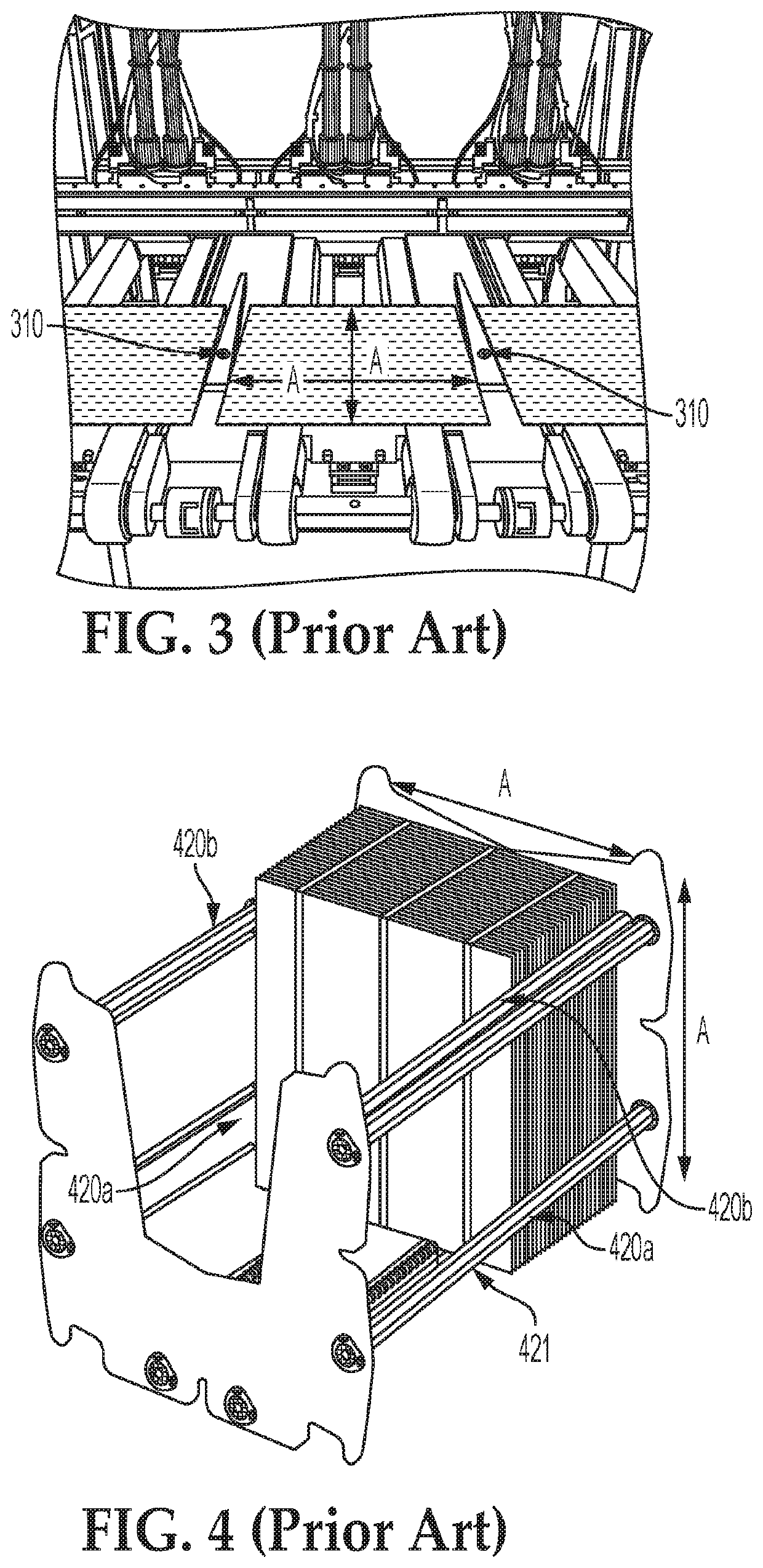
[0071]Certain processing schemes and architecture are disclosed in U.S. Pat. No. 8,293,009B2, titled Methods For Efficiently Making Thin Semiconductor Bodies From Molten Material For Solar Cells and the Like, inventors Emanuel M. Sachs et al., assigned to 1366 Technologies Inc., which issued on Oct. 23, 2012, and additional patents related thereto, including U.S. Pat. No. 8,696,810, issued on Apr. 15, 2014 and U.S. Pat. No. 9,643,342, issued on May 9, 2017. The above-mentioned patent disclosures are hereby incorporated fully herein by reference. The technology disclosed in the above referenced patents is referred to herein collectively as Direct Wafer (DW) technology.

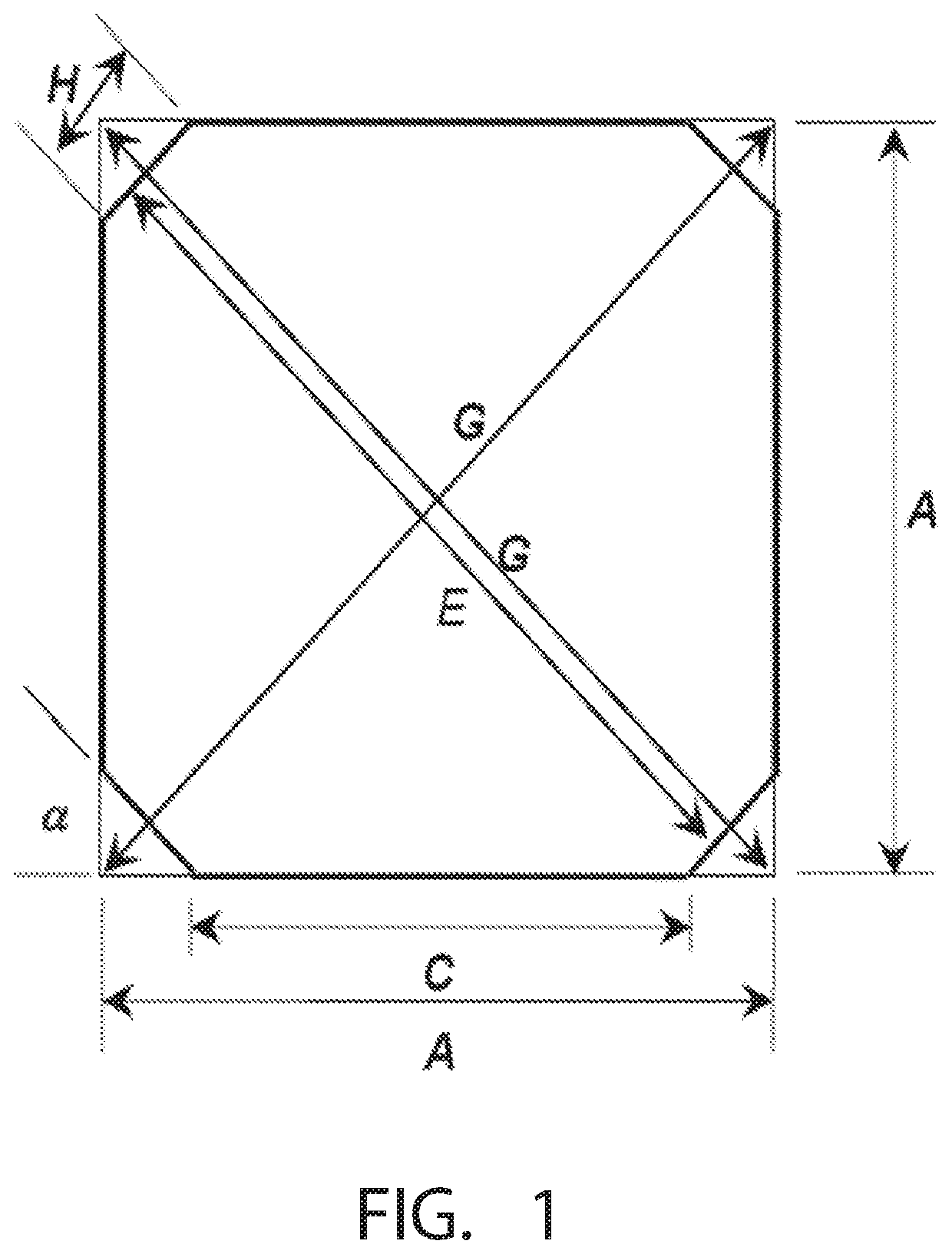
[0072]Aspects of the invention disclosed herein relate to wafers that are of an industry standard size along one dimension, referred to herein as their width w, and which are longer along the dimension that is perpendicular to the standard size width, referred to herein as the wafer's length nL. The industry standard re...


PUM

PropertyMeasurementUnit
length sizeaaaaaaaaaa
sizeaaaaaaaaaa
sizeaaaaaaaaaa

Abstract

A semiconductor wafer is as wide as the industry standard width A (presently 156 mm+/−1 mm) and is longer than the industry standard A by at least 1 mm and as much as the standard equipment can reasonably accommodate, presently approximately 3-20 mm and potentially longer, thus, gaining significant additional surface area for sunlight absorption. Modules may be composed of a plurality of such larger wafers. Such wafers can be processed in conventional processing equipment that has a wafer retaining portion of industry standard size A and a configuration that also accommodates a wafer with a perpendicular second edge longer than A by at least 1 and typically 3-20 mm. Wet bench carriers and transport and inspection stations can be so used.

Description

CROSS-REFERENCE TO RELATED APPLICATIONS[0001]This claims priority to U.S. Provisional application No. 62 / 576,143, filed on Oct. 24, 2017, entitled SEMI-CONDUCTOR WAFERS FOR USE IN SOLAR CELLS AND MODULES THAT ARE LONGER THAN SIZE OF A SIDE OF THE INDUSTRY STANDARD SQUARE, AND METHODS OF MAKING AND USING SAME AND SOLAR CELLS AND MODULES INCORPORATING SAME, the full disclosure of which is fully incorporated by reference, herein.BACKGROUND[0002]Wafers that are used in solar cells and solar modules are generally square. They are manufactured in squares, which are trimmed to a final size, and used in that shape. Alternatively, in some cases, they are manufactured in the square shape, and then are cut into smaller units which are arranged in such a way to expose most if not all of the surface area of the manufactured wafer to the sun, but to also reduce other losses that arise if the full squares are used in their original shapes.[0003]The standards for wafers for the Photovoltaic industr...

Claims


Application Information

Patent Timeline
Patent Type & Authority Applications(United States)
IPC IPC(8): H01L21/673H01L21/677H01L31/0352H01L31/18B65G47/90
CPCH01L31/1876H01L21/67706H01L21/6734B65G47/90H01L31/035281H01L21/67313H01L31/042H01L31/1804Y02E10/547Y02P70/50H01L21/67353H01L21/67373
Inventor STEEMAN, ROBERTUS ANTONIUS
Owner CUBICPV INC
Why Eureka
Try Eureka