Manufacturing method of OLED display panel

Inactive Publication Date: 2020-09-24
SHENZHEN CHINA STAR OPTOELECTRONICS SEMICON DISPLAY TECH CO LTD
View PDF0 Cites 1 Cited by
  • Summary
  • Abstract
  • Description
  • Claims
  • Application Information

AI Technical Summary

Benefits of technology

The present patent improves the manufacturing process of OLED display panels by using a protective layer to remove any residue or foreign particles from the pixel aperture during the formation of a pixel. This ensures that ink material for printing on the anode layer in the pixel aperture can spread out fully, which prevents uneven lighting and improves the display effect and performance of OLED display panels. Extending the service life of OLED display panels is also achieved by this improved manufacturing process.

Problems solved by technology

However, material utilization is low using the full-evaporation technology so to manufacture a device with a high resolution is a difficult task.
On the other hand, the cost of manufacturing the OLED device using the printing technology is about 17% lower compared with the whole deposition technology.
Accordingly, the OLED display panel not only emits light unequally but also shows mura like bright or dark spots, which seriously affects the display effect and service life of the OLED display panel.
In summary, some problems occur when the organic functional layer is printed on the anode layer of the light emitting area in the manufacturing process of the OLED display panel.
The problems are that the organic functional ink material fails to be spread completely, and thereby, the display effect of the OLED display panel is very poor and the service life is short.
The technical problem of the related art that the display effect and the service life of an OLED display panel are not influenced by unsuccessful spreading of ink materials when an organic functional film is printed on the anode layer.

Method used


Image

  • Manufacturing method of OLED display panel
  • Manufacturing method of OLED display panel
  • Manufacturing method of OLED display panel

Examples


Embodiment Construction

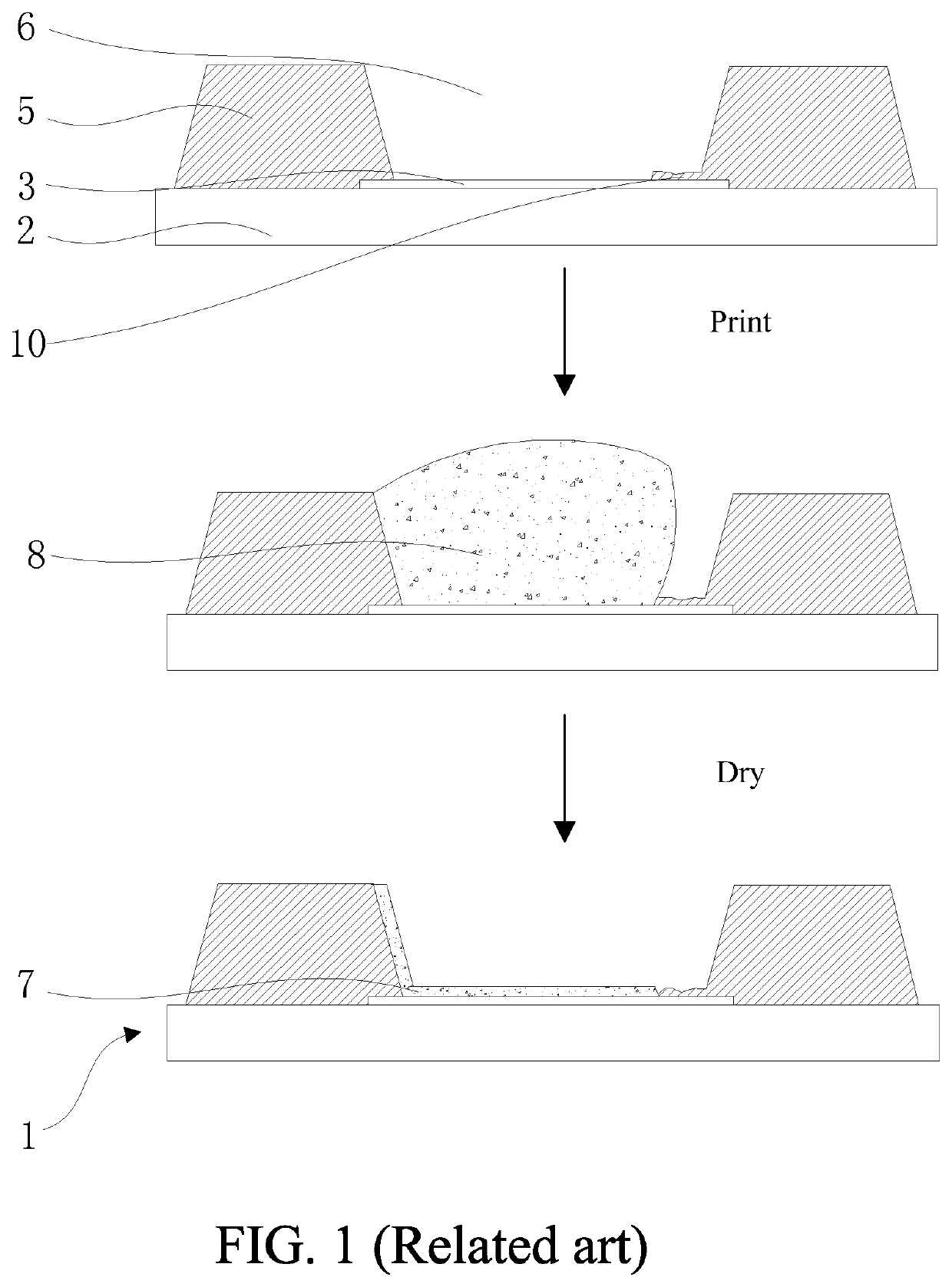
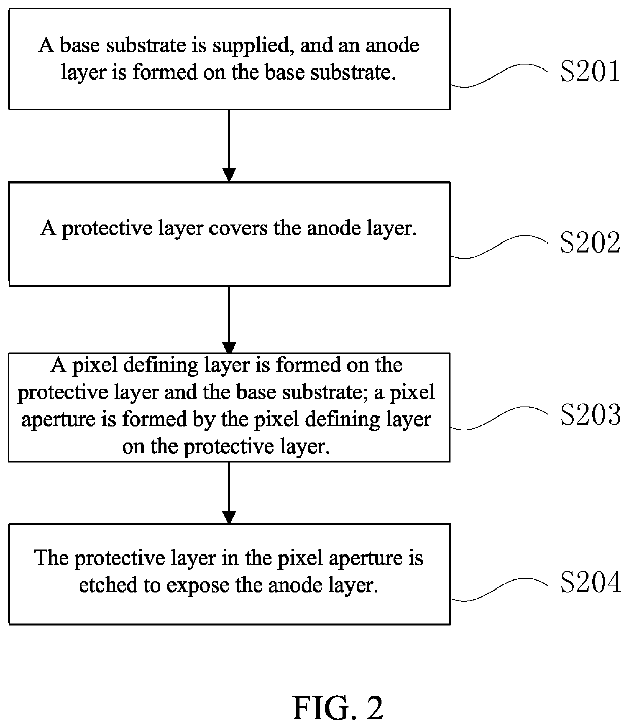
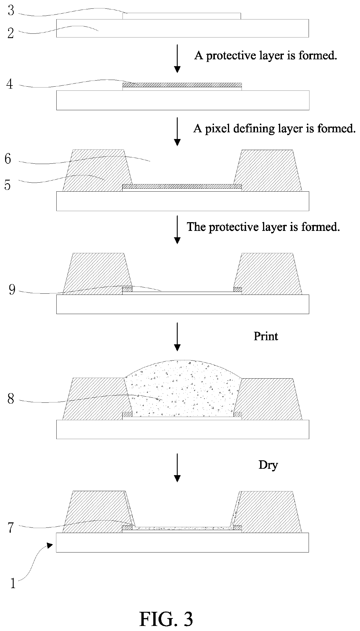
[0030]The embodiments of the present disclosure are described in detail hereinafter. Examples of the described embodiments are given in the accompanying drawings, wherein the identical or similar reference numerals constantly denote the identical or similar elements or elements having the identical or similar functions. The specific embodiments described with reference to the attached drawings are all exemplary and are intended to illustrate and interpret the present disclosure, which shall not be construed as causing limitations to the present disclosure.

[0031]In the description of the present disclosure, it should be understood that terms such as “center,”“longitudinal,”“lateral,”“length,”“width,”“thickness,”“upper,”“lower,”“front,”“rear,”“left,”“right,”“vertical,”“horizontal,”“top,”“bottom,”“inside,”“outside,”“clockwise,”“counter-clockwise” as well as derivative thereof should be construed to refer to the orientation as then described or as shown in the drawings under discussion....


PUM


Abstract

A manufacturing method of an organic light emitting diode (OLED) display panel, includes: supplying a base substrate, forming an anode layer on the base substrate, covering a protective layer on the protective layer, forming a pixel defining layer on the protective layer and the base substrate, enclosing the pixel defining layer as a pixel aperture on the protective layer, and etching the protective layer in the pixel aperture to expose the anode layer.

Description

BACKGROUND1. Field of the Disclosure[0001]The present disclosure relates to the field of display panel, and more particularly, to a manufacturing method of an organic light emitting diode (OLED) display panel.2. Description of the Related Art[0002]Statements here only provide background information related to the present disclosure, without necessarily constituting the related art.[0003]The main method for manufacturing an organic light emitting diode (OLED) device deposition and printing. Nowadays, the use of full-evaporation process for the manufacturing of an OLED display in large and small sizes with respect to the printing technology is quite mature so the OLED display has been commercially manufactured. However, material utilization is low using the full-evaporation technology so to manufacture a device with a high resolution is a difficult task. The material utilization is up to 90% using the printing technology for manufacturing the OLED device. On the other hand, the cost o...

Claims


Application Information

Patent Timeline
IPC IPC(8): H01L51/56H01L51/00H01L51/52
CPCH01L51/56H01L51/0017H01L51/5253H01L2251/308H01L2251/306H01L51/003H10K59/122H10K59/173H10K71/13H10K71/231H10K71/00H10K59/873H10K50/844H10K71/80H10K2102/102H10K2102/103
Inventor LIU, HUALONG
Owner SHENZHEN CHINA STAR OPTOELECTRONICS SEMICON DISPLAY TECH CO LTD
Why Eureka
Try Eureka