

Power semiconductor module with power semiconductor switches
- Summary
- Abstract
- Description
- Claims
- Application Information
AI Technical Summary
Benefits of technology
Problems solved by technology
Method used
Image

Examples
Embodiment Construction
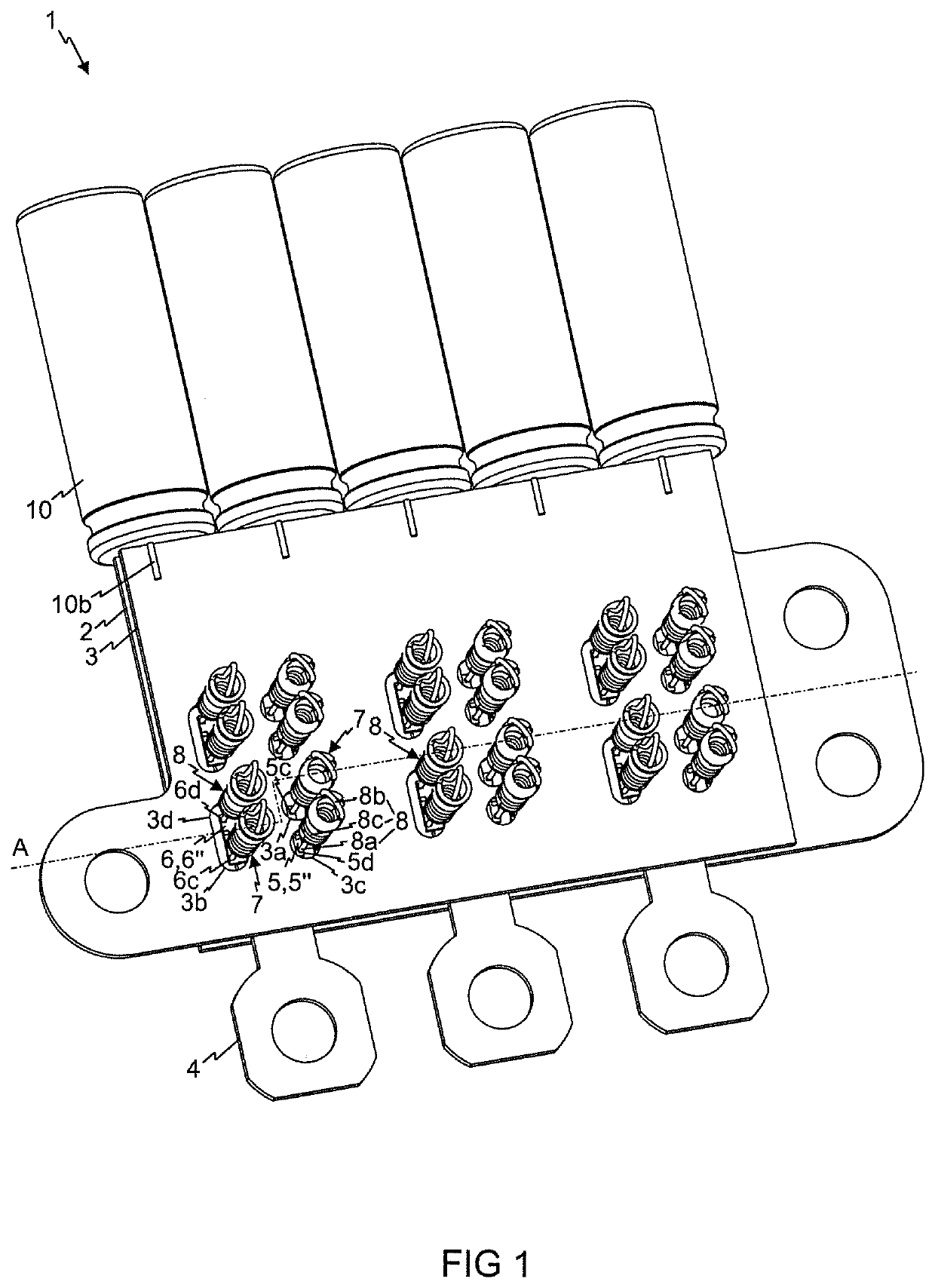
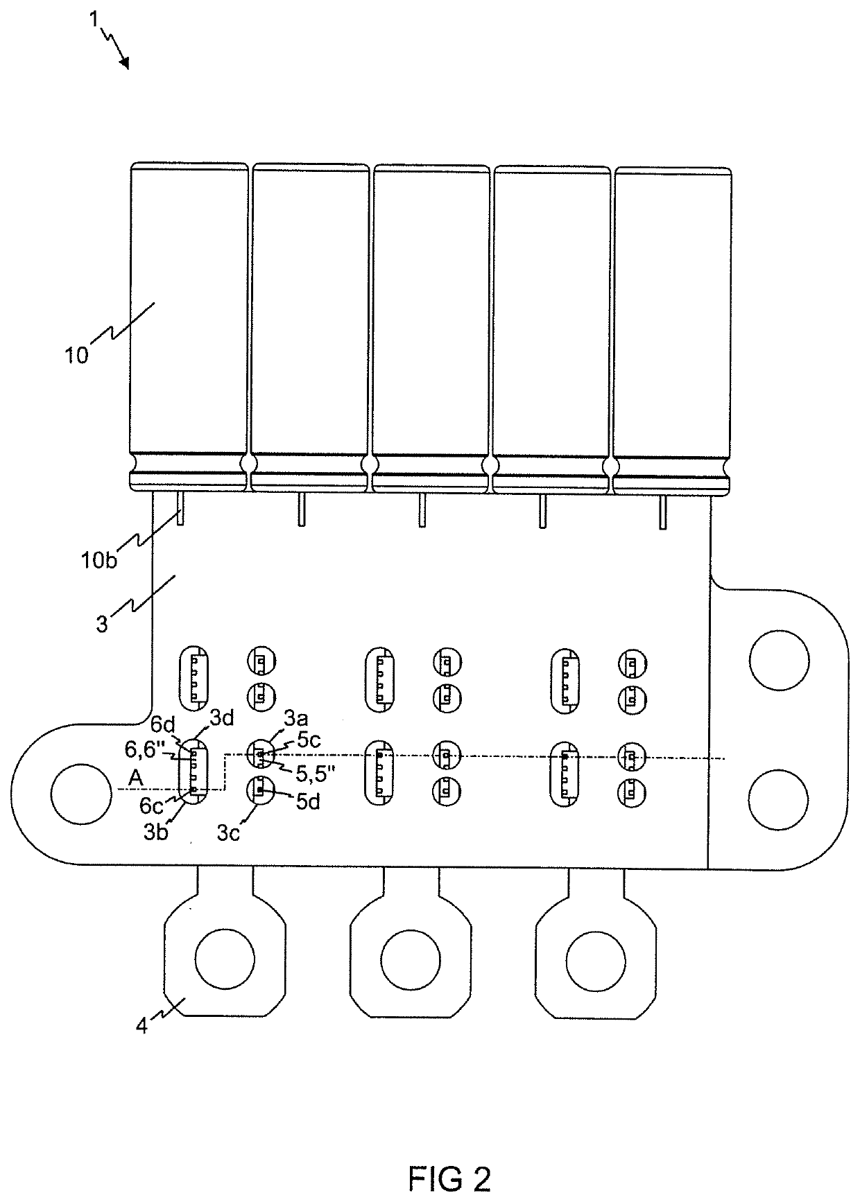
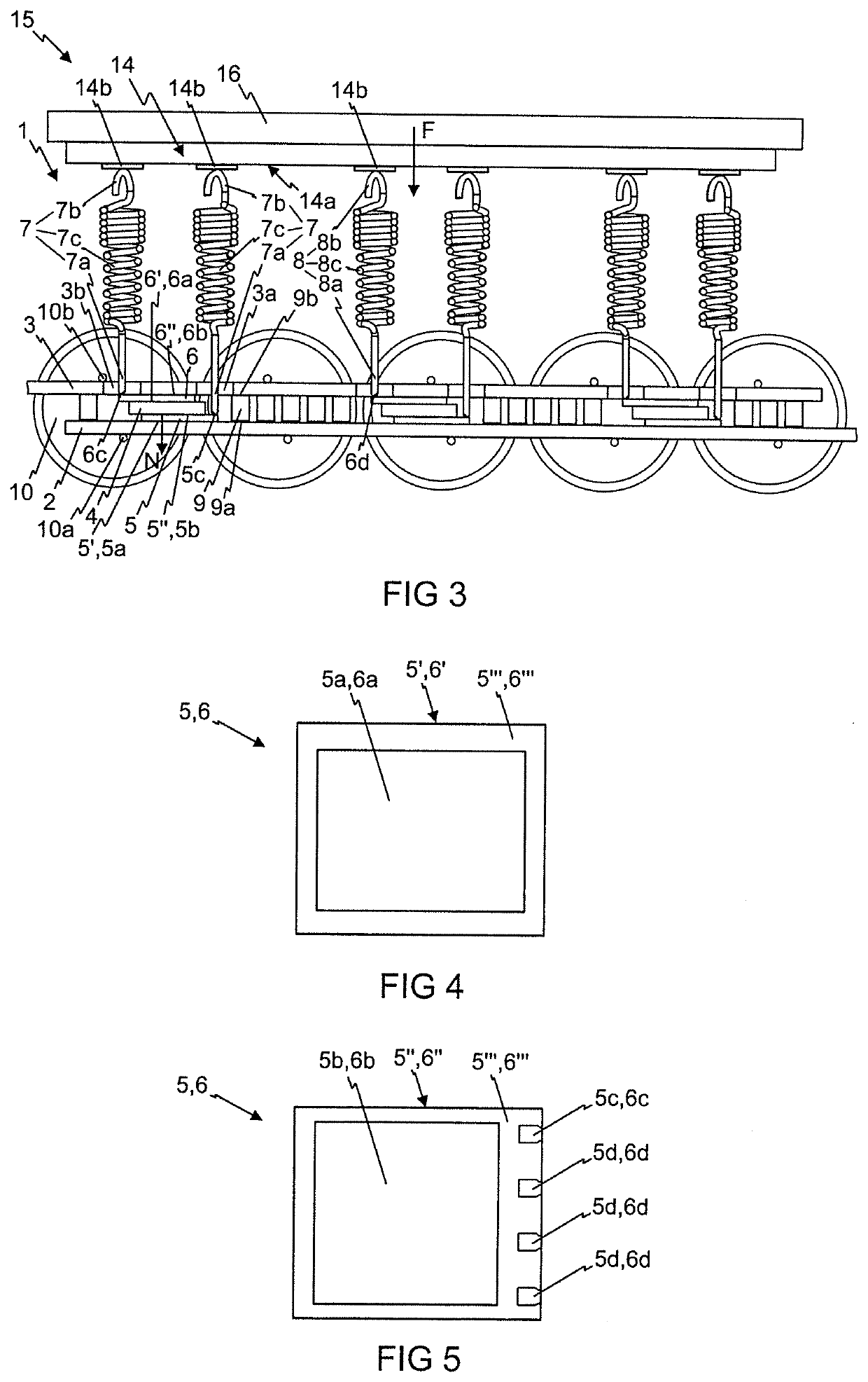
[0027]Reference will now be made in detail to embodiments of the invention. Wherever possible, same or similar reference numerals are used in the drawings and the description to refer to the same or like parts or steps. The drawings are in simplified form and are not to precise scale. The word ‘couple’ or ‘link’ or ‘connect’ and similar terms do not necessarily denote direct and immediate connections, but also include connections through intermediate elements or devices. For purposes of convenience and clarity only, directional (up / down, etc.) or motional (forward / back, etc.) terms may be used with respect to the drawings. These and similar directional terms should not be construed to limit the scope in any manner. It will also be understood that other embodiments may be utilized without departing from the scope of the present invention, and that the detailed description is not to be taken in a limiting sense, and that elements may be differently positioned, or otherwise noted as in...
PUM
 Abstract
Description
Claims
Application Information