Thin film transistor and electrical circuit
- Summary
- Abstract
- Description
- Claims
- Application Information
AI Technical Summary
Benefits of technology
Problems solved by technology
Method used
Image

Examples
Embodiment Construction
[0062]In the present specification, the specific feature, structure, material, or characteristic described may be in combination in a suitable manner in any one or more of the embodiments or examples. In addition, it will be apparent to those skilled in the art that different embodiments or examples described in this specification, as well as features of different embodiments or examples, may be combined without contradictory circumstances.
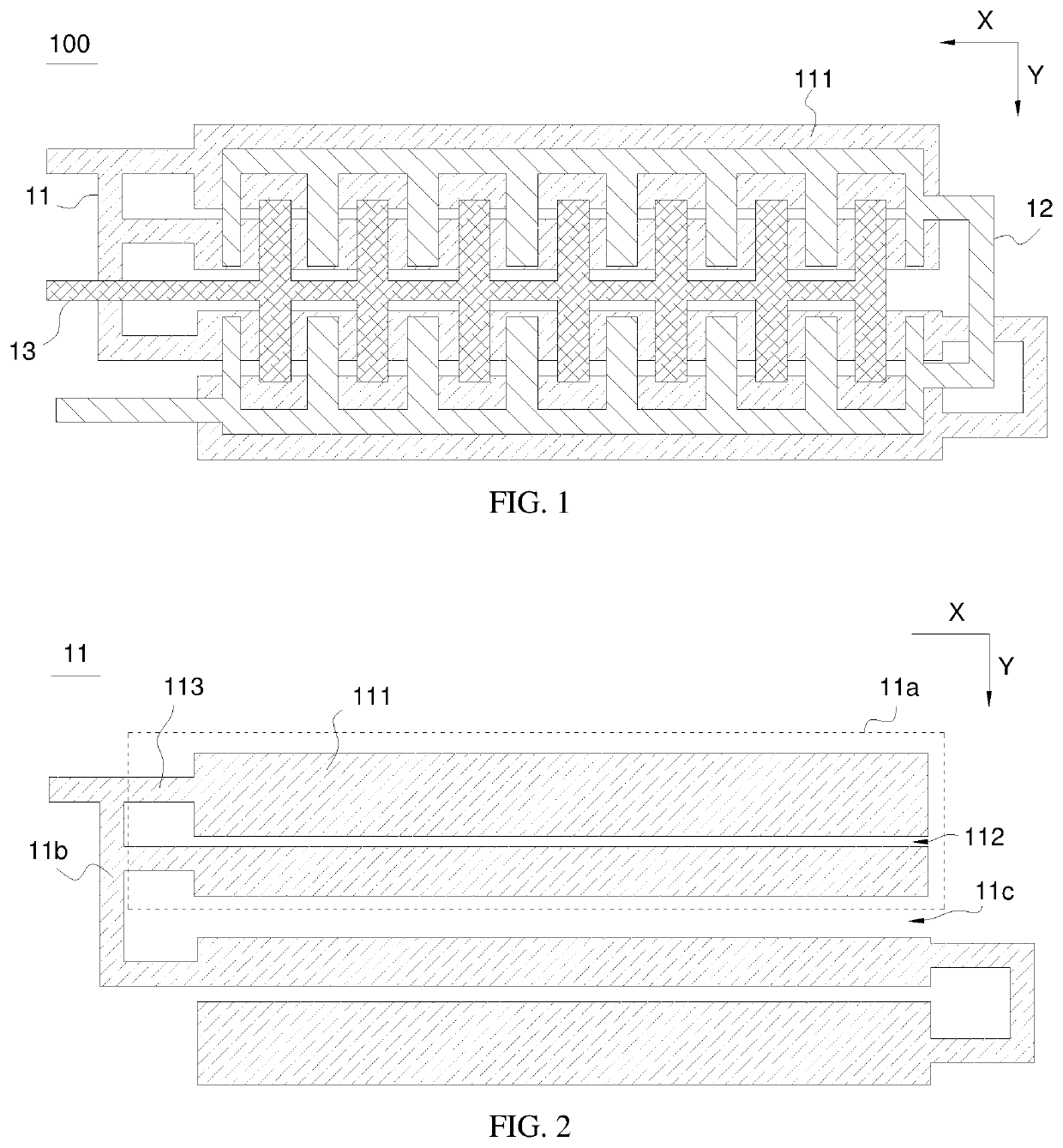
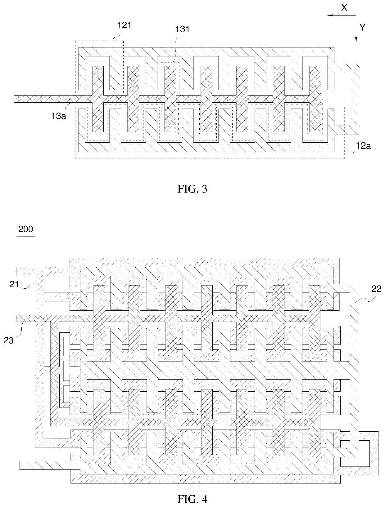
[0063]Please refer to FIG. 1, FIG. 2, and FIG. 3. FIG. 1 is a schematic diagram of a thin film transistor (TFT) according to a first embodiment of the present disclosure. FIG. 2 is a schematic diagram of a gate 11 of the TFT according to the first embodiment. FIG. 3 is a schematic diagram of a source / drain layer of the TFT of the first embodiment. The TFT 10 includes the gate 11 and the source / drain layer. The source / drain layer includes a source 12 and a drain 13. The gate 11 is insulated from the source / drain layer. The gate 11 is arranged above...
PUM
 Abstract
Description
Claims
Application Information