
Band gap engineered materials

Active Publication Date: 2021-03-04
WESTERN MICHIGAN UNIVERSITY
View PDF0 Cites 0 Cited by
  • Summary
  • Abstract
  • Description
  • Claims
  • Application Information

AI Technical Summary

Benefits of technology

The present patent discloses a method for fabricating semiconductor materials with desired band gaps and controlling the band gap energy through variation of process parameters. This method can be used to tune the band gap of semiconductor materials for various applications such as light-emitting diodes, junction transistors, solar cells, and tunnel diodes. The method can also be used to control the transition temperature of superconductor materials. The patent provides a predefined correlation between the band gap and the stoichiometry of semiconductor materials and an order parameter to determine the required band gap energy. The process parameters can be controlled to form semiconductor devices with the desired band gap energy.

Problems solved by technology

Disorder is known to affect the band gap.

Method used


Image

  • Band gap engineered materials
  • Band gap engineered materials
  • Band gap engineered materials

Examples


Embodiment Construction

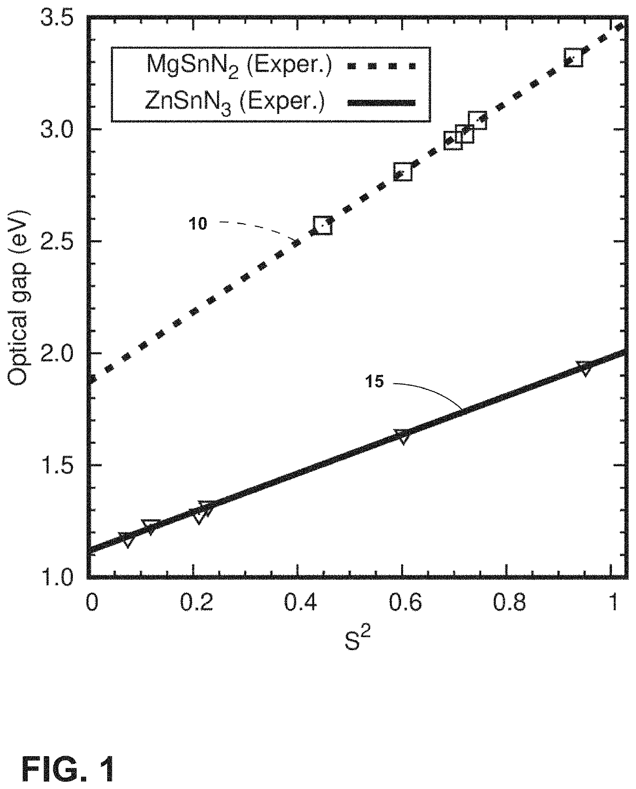
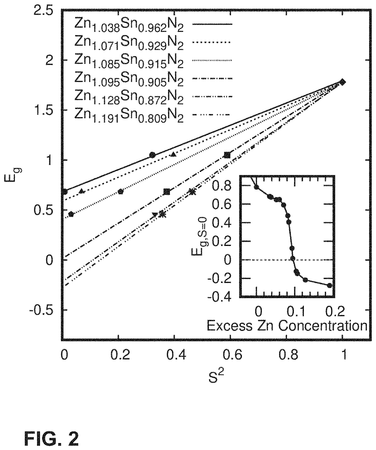
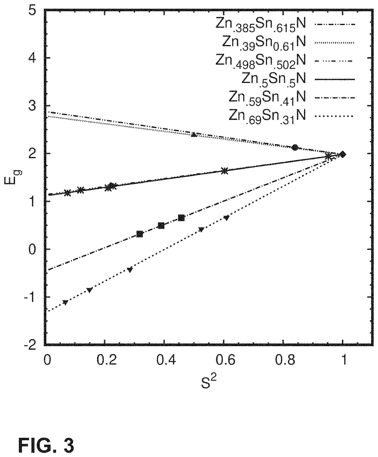
[0043]Conventional approaches to band gap engineering may not recognize the full range of achievable bandgap values. However, as discussed in more detail below, the present disclosure provides a way to accomplish a full range of band gaps in the context of structural motifs as viewed quantitatively with the assistance of an appropriately constructed model of lattice disorder (e.g., an order parameter). It will be understood that “different material compositions” (e.g. different semiconductor material compositions) as used herein generally encompasses differences in stoichiometry and differences in the elemental composition of the material.

[0044]In an otherwise interstitial-free lattice, the set of structural motifs that arise from disorder are defined through the range of possible anti-site defects. Since such defects can have large energies of formation, it may be argued that they are unlikely to form in lattices. A disordered lattice, however, has a higher entropy than a perfectly...


PUM


Abstract

A process of fabricating semiconductor devices includes determining a correlation between band gap and long range order parameter for one or more stoichiometries. Semiconductor materials having a preselected (target) band gap can be fabricated by controlling process parameters to form a material having a stoichiometry and long range order parameter having the target band gap.

Description

CROSS-REFERENCE TO RELATED APPLICATION[0001]This application claims the benefit under 35 U.S.C. § 119(e) to U.S. Provisional Patent Application No. 62 / 895,678, filed Sep. 4, 2019, entitled “BAND GAP ENGINEERED MATERIALS,” which is incorporated herein by reference in its entirety.STATEMENT REGARDING FEDERALLY SPONSORED RESEARCH OR DEVELOPMENT[0002]This invention was made, in part, with government support under DMR-1410915 awarded by the NSF. The government has certain rights in the invention.BACKGROUND OF THE INVENTION[0003]Variations in the band gap of semiconducting materials affect various electrical characteristics of the material. In general, the band gap is the energy difference between the valence band maximum and the conduction band minimum. Various approaches to control or modify the band gap of semiconductor materials have been developed.[0004]In general, an order parameter is a measure of changes following a phase transition. In the case of binary alloys, a degree of order...

Claims


Application Information

Patent Timeline
IPC IPC(8): H01L29/66H01L21/66
CPCH01L29/66893H01L22/14H01L29/737H01L29/24H01L22/12H01L22/20H10N60/01H10N60/0912H10N60/12
Inventor MAKIN, III, ROBERT A.DURBIN, STEVEN MICHAEL
Owner WESTERN MICHIGAN UNIVERSITY
Learn More