

Circuit member joint structure and circuit member joining method
a technology of circuit member and joint structure, which is applied in the direction of printed circuit non-printed electric components association, printed circuit details, non-metallic protective coating application, etc., can solve the problems of particularly prone to reliability compromise, physical joint and electrical connection reliability might be compromised, etc., to achieve high reliability of electrical connection and physical joint high reliability
- Summary
- Abstract
- Description
- Claims
- Application Information
AI Technical Summary
Benefits of technology
Problems solved by technology
Method used
Image

Examples
first preferred embodiment
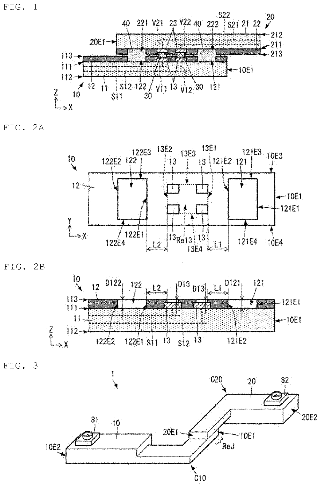
[0034]A circuit member joint structure and a circuit member joining method according to a first preferred embodiment of the present invention will be described with reference to the drawings. FIG. 1 is a side sectional view of a joint structure for circuit members 10 and 20, according to the first preferred embodiment. FIG. 2A is a plan view illustrating a configuration of a joint portion in the circuit member 10, and FIG. 2B is a side sectional view of the same.
[0035]The circuit member joint structure illustrated in FIG. 1 includes the circuit member 10 and the circuit member 20. The joint structure of the circuit members 10 and 20 further includes a conductive joining material 30 and an insulating joining material 40. The circuit member 10 corresponds to a “first circuit member”, and the circuit member 20 corresponds to a “second circuit member”.
[0036]The circuit member 10 and the circuit member 20 are, for example, circuit boards. The circuit member 10 and the circuit member 20 c...
second preferred embodiment
[0117]Next, a circuit member joint structure according to a second preferred embodiment of the present invention will be described with reference to the drawings. FIG. 9 is a plan view illustrating a configuration of a joint portion of circuit members.
[0118]As illustrated in FIG. 9, a circuit member 10A in the circuit member joint structure according to the second preferred embodiment is different from the circuit member 10 according to the first preferred embodiment in that a recess 121A and a recess 122A are provided. Other configurations of the circuit member 10A are the same or substantially the same as those of the circuit member 10, and the description of the same or similar portions will be omitted. Although not shown in FIG. 9, a circuit member 20A (only the outer shape of which is illustrated in FIG. 9) has the same or substantially the same configuration as the circuit member 10A.
[0119]The recess 121A extends over the entirety or substantially the entirety of the protectiv...
third preferred embodiment
[0121]Next, a circuit member joint structure according to a third preferred embodiment of the present invention will be described with reference to the drawings. FIGS. 10A and 10B are plan views illustrating a configuration of a joint portion in circuit members 10B and 10B1.
[0122]As illustrated in FIG. 10A, the circuit member 10B in the circuit member joint structure according to the third preferred embodiment is different from the circuit member 10 according to the first preferred embodiment in that a recess 120 is provided. Other configurations of the circuit member 10B are the same or substantially the same as those of the circuit member 10, and the description of the same or similar portions will be omitted. Although not shown in FIG. 1A, a circuit member 20B (only the outer shape of which is illustrated in FIG. 10A) has the same or substantially the same configuration as the circuit member 10B.
[0123]The recess 120 has a shape that surrounds the mounting region Re13. That is, th...
PUM
 Abstract
Description
Claims
Application Information