
Semiconductor package structure and manufacturing method thereof

a technology of semiconductors and packaging, applied in the direction of semiconductor devices, electrical equipment, radio frequency controlled devices, etc., can solve the problems of difficulty in making a package thickness thinner, and achieve the effect of reducing the possibility and making the package thickness thinner

Active Publication Date: 2021-04-01
POWERTECH TECHNOLOGY
View PDF11 Cites 4 Cited by
  • Summary
  • Abstract
  • Description
  • Claims
  • Application Information

AI Technical Summary

Benefits of technology

The invention provides a way to make semiconductor packages thinner and reduce the likelihood that the image recognition is affected by the underfill used in the process. This is achieved by using a dam structure on the substrate that surrounds the image sensing area and prevents the underfill from overflowing into that area. This allows for a thinner package and reduces the possibility of image recognition issues caused by the underfill.

Problems solved by technology

For instance, how to make a package thickness thinner has become a challenge.

Method used


Image

  • Semiconductor package structure and manufacturing method thereof
  • Semiconductor package structure and manufacturing method thereof
  • Semiconductor package structure and manufacturing method thereof

Examples


Embodiment Construction

[0014]Reference will now be made in detail to the present preferred embodiments of the invention, examples of which are illustrated in the accompanying drawings. Wherever possible, the same reference numbers are used in the drawings and the description to refer to the same or like parts.

[0015]Directional terminology (e.g., top, down, right, left, front, rear, top, and bottom) is used with reference to the orientation of the Figure(s) being described. As such, the directional terminology is used for purposes of illustration and is in no way limiting.

[0016]Unless otherwise clearly indicated, the method in this disclosure should not be construed as requiring steps therein to be performed in a particular order.

[0017]The invention will be described more comprehensively below with reference to the drawings for the embodiments. However, the invention may also be implemented in different forms rather than being limited by the embodiments described in the invention. Thicknesses, dimensions a...


PUM

PropertyMeasurementUnit
ambient pressureaaaaaaaaaa
conductiveaaaaaaaaaa

Abstract

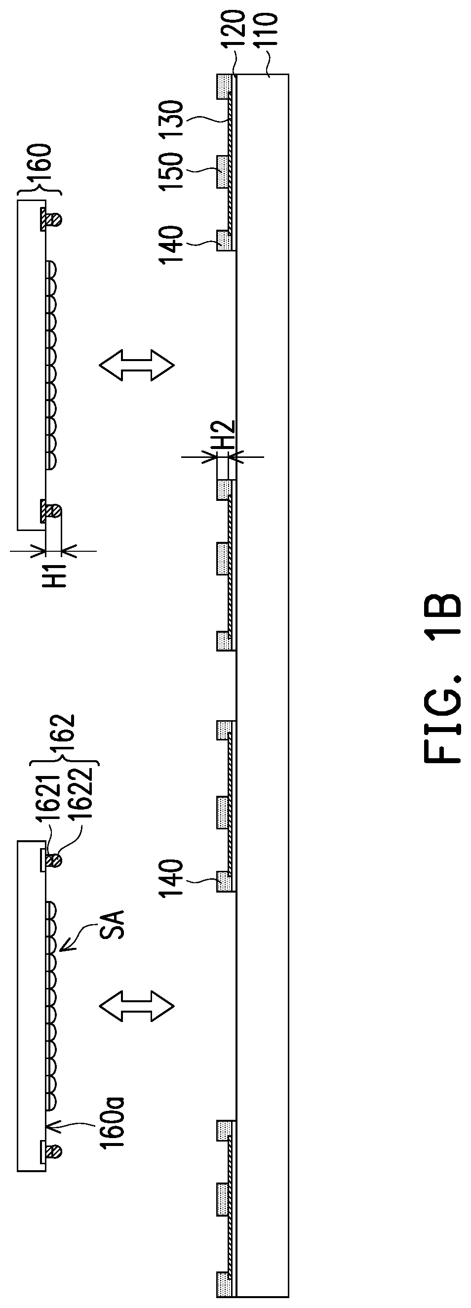
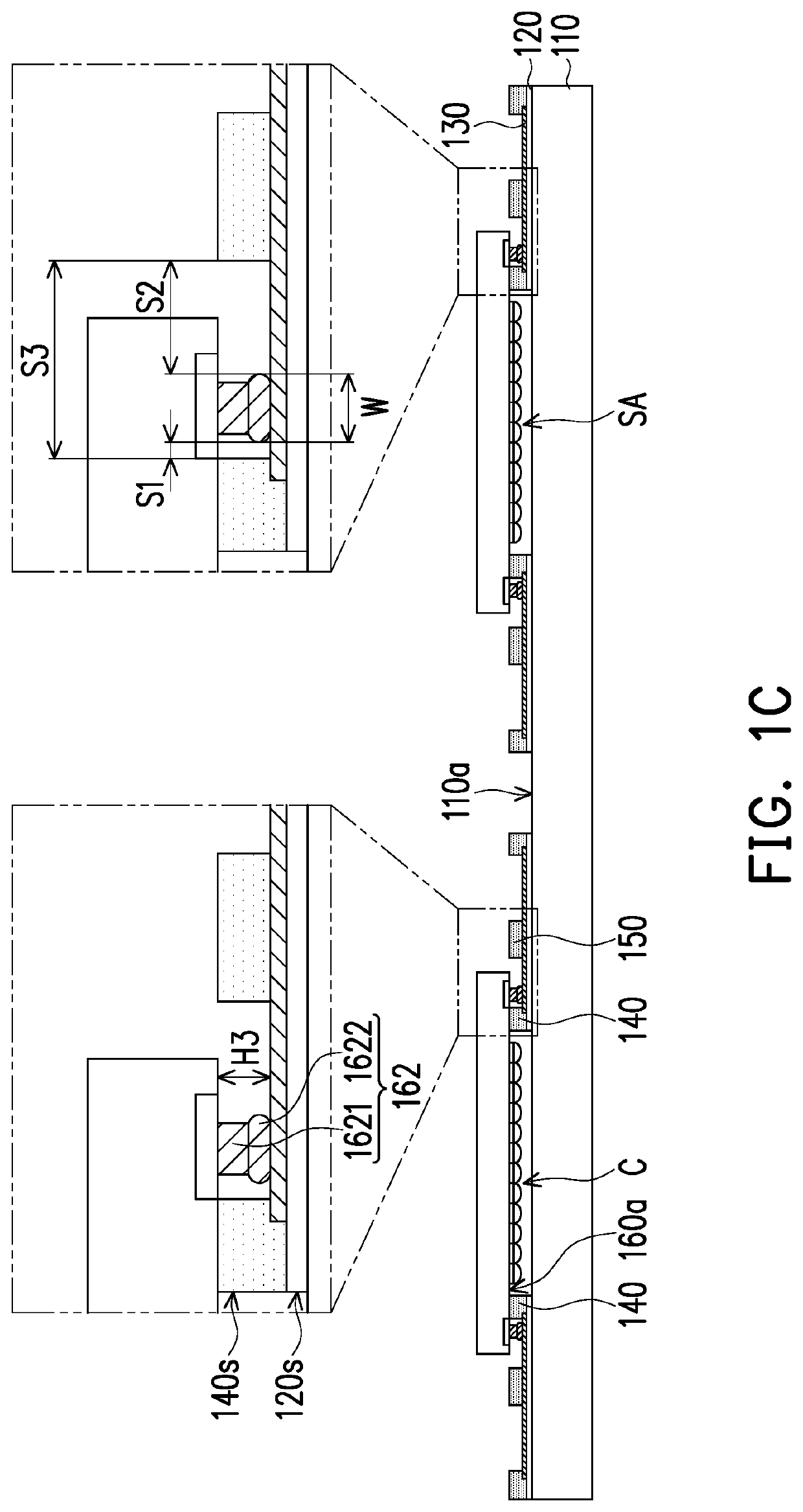
A semiconductor package structure including a sensor die, a substrate, a light blocking layer, a circuit layer, a dam structure and an underfill is provided. The sensor die has a sensing surface. The sensing surface includes an image sensing area and a plurality of conductive bumps. The substrate is disposed on the sensing surface. The light blocking layer is located between the substrate and the sensor die. The circuit layer is disposed on the light blocking layer. The sensor die is electrically connected to the circuit layer by the conductive bumps. The dam structure is disposed on the substrate and surrounds the image sensing area. Opposite ends of the dam structure directly contact the sensor die and the light blocking layer. The underfill is disposed between the dam structure and the conductive bumps.

Description

CROSS-REFERENCE TO RELATED APPLICATION[0001]This application claims the priority benefit of Taiwan application serial no. 108135048, filed on Sep. 27, 2019. The entirety of the above-mentioned patent application is hereby incorporated by reference herein and made a part of this specification.BACKGROUNDField of the Invention[0002]The invention relates to a semiconductor package structure and a manufacturing method thereof, and more particularly, to a semiconductor package structure having a dam structure and a manufacturing method thereof.Description of Related Art[0003]In order to make electronic products design light, thin, short and small, semiconductor packaging technology is continuing to improve, in an attempt to develop products that are smaller, lighter, more integrated, and more competitive in the market. For instance, how to make a package thickness thinner has become a challenge.SUMMARY[0004]The invention provides a semiconductor package structure and a manufacturing metho...

Claims


Application Information

Patent Timeline
Patent Type & Authority Applications(United States)
IPC IPC(8): H01L27/146
CPCH01L27/14618H01L27/14623H01L27/14698H01L27/14685H01L27/14636
Inventor HSU, HUNG-HSINCHANG, WEN-HSIUNG
Owner POWERTECH TECHNOLOGY
Learn More