
Display device and method of manufacturing display device

a display device and display device technology, applied in the direction of semiconductor devices, basic electric elements, electrical appliances, etc., can solve the problems of narrow space for arranging the pixel circuit, and achieve the effect of increasing the capacitance of the capacitor and reducing the threshold voltage of the second transistor

Inactive Publication Date: 2021-05-13
SAMSUNG DISPLAY CO LTD
View PDF0 Cites 2 Cited by
  • Summary
  • Abstract
  • Description
  • Claims
  • Application Information

AI Technical Summary

Benefits of technology

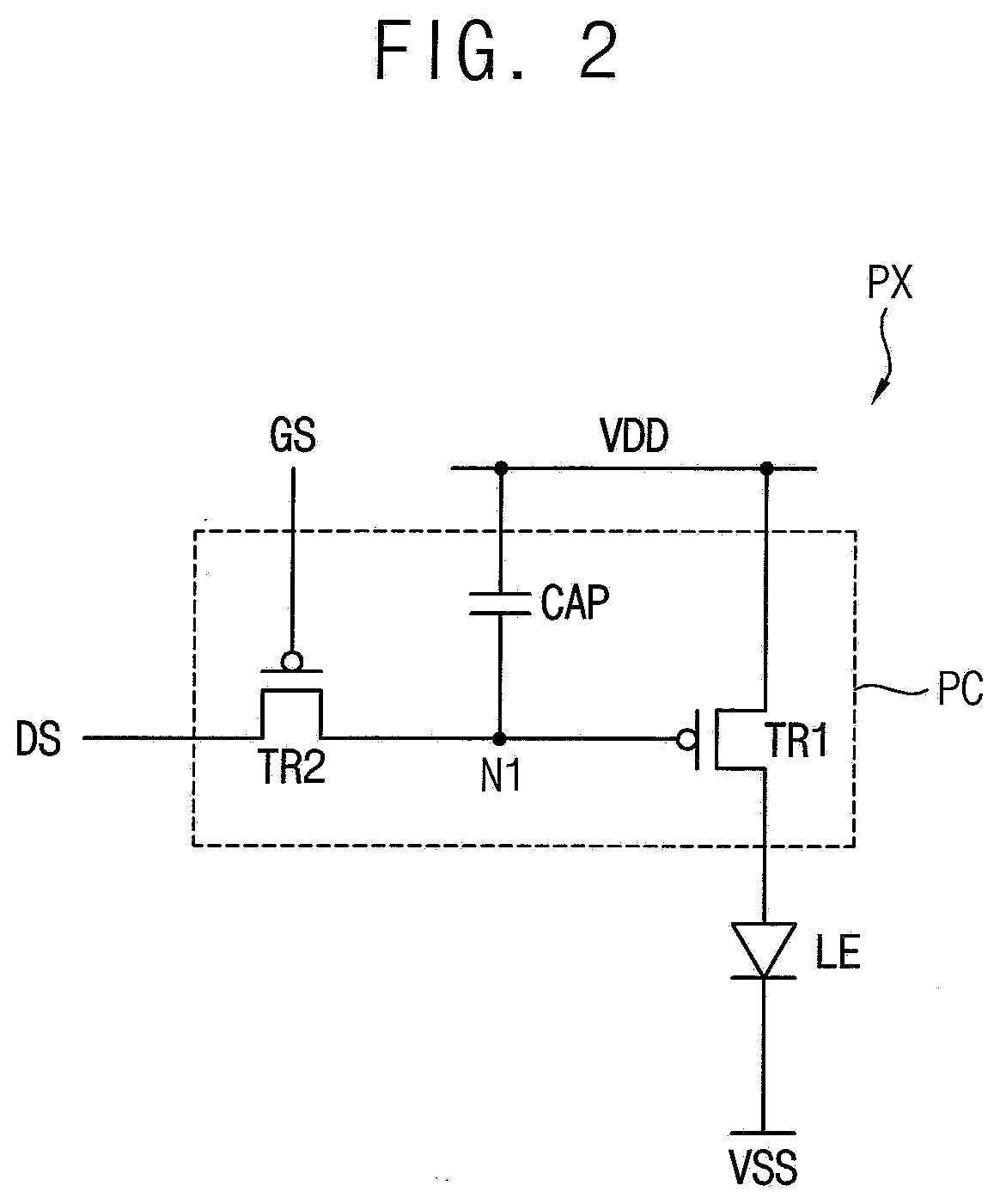
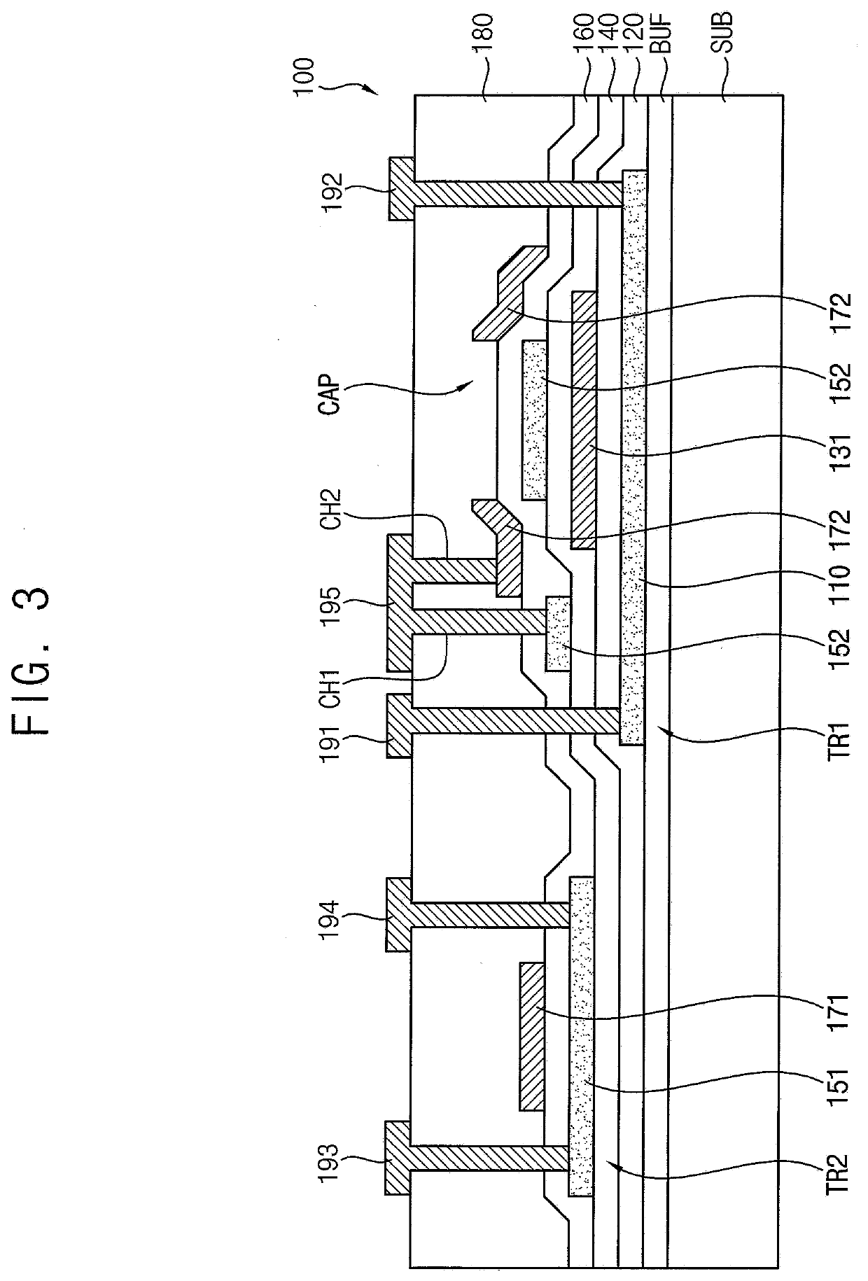
This patent provides a display device that has improved characteristics and a manufacturing process that reduces costs and time. The device includes a second transistor and a capacitor, with the second transistor having a decreased threshold voltage and the capacitor having an increased capacitance. The manufacturing process simultaneously disposes the second active layer of the second transistor and the first capacitor electrode of the capacitor on the insulation layer, reducing the number of photolithography processes required.

Problems solved by technology

Recently, with the development of high resolution display devices, the space for arranging the pixel circuit has become narrow.

Method used


Image

  • Display device and method of manufacturing display device
  • Display device and method of manufacturing display device
  • Display device and method of manufacturing display device

Examples


Embodiment Construction

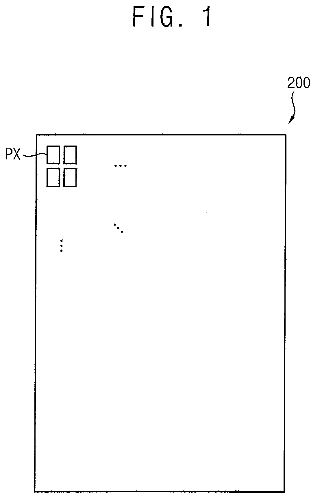
[0056]Hereinafter, display devices and methods of manufacturing display devices in accordance with embodiments will be explained in detail with reference to the accompanying drawings.

[0057]In the drawing figures, dimensions may be exaggerated for clarity of illustration.

[0058]As used herein, the singular forms “a,”“an,” and “the” are intended to include the plural forms as well, unless the context clearly indicates otherwise. The term “and / or” is intended to include any combination of the terms “and” and “or” for the purpose of its meaning and interpretation. For example, “A and / or B” may be understood to mean “A, B, or A and B.” The terms “and” and “or” may be used in the conjunctive or disjunctive sense and may be understood to be equivalent to “and / or.”

[0059]The term overlap may include layer, stack, face or facing, extending over, extending under, covering or partly covering or any other suitable term as would be appreciated and understood by those of ordinary skill in the art. ...


PUM

PropertyMeasurementUnit
permittivityaaaaaaaaaa
semiconductoraaaaaaaaaa
constant voltageaaaaaaaaaa

Abstract

A display device includes a substrate, a first active layer on the substrate, a first insulation layer on the first active layer, a first gate electrode on the first insulation layer, the first gate electrode overlapping the first active layer, a second insulation layer on the first gate electrode, a second active layer on the second insulation layer, a first capacitor electrode on the second insulation layer, the first capacitor electrode overlapping the first gate electrode, a third insulation layer on the second active layer and the first capacitor electrode, a second gate electrode on the third insulation layer, the second gate electrode overlapping the second active layer, and a second capacitor electrode on the third insulation layer, the second capacitor electrode overlapping the first gate electrode and electrically connected to the first capacitor electrode.

Description

CROSS-REFERENCE TO RELATED APPLICATION(S)[0001]This application claims priority to and benefits of Korean Patent Application No. 10-2019-0142684 under 35 U.S.C. §119, filed in the Korean Intellectual Property Office (KIPO) on Nov. 8, 2019, the entire contents of which are incorporated herein by reference.BACKGROUNDTechnical Field[0002]Embodiments relate to a display device including a display substrate that includes a transistor and a capacitor, and a method of manufacturing the display device.Description of the Related Art[0003]Display devices are devices that display an image for providing visual information to a user. Recently, an organic light emitting display device has attracted attention among the display devices.[0004]The organic light emitting display device has a self-luminous characteristics and, unlike a liquid crystal display device, does not require a separate light source, thereby reducing thickness and weight. The organic light emitting display device exhibits high q...

Claims


Application Information

Patent Timeline
Patent Type & Authority Applications(United States)
IPC IPC(8): H01L27/12
CPCH01L27/1255H01L27/1274H01L27/1222H10K59/123H10K59/1213H10K59/1216H10K59/122H01L27/124H01L27/1214H10K59/124H10K50/80H10K71/00
Inventor KIM, JAY BUMKIM, MYEONG HOSON, KYOUNG SEOKLEE, SEUNG JUNLEE, SEUNG HUNLIM, JUN HYUNG
Owner SAMSUNG DISPLAY CO LTD
Learn More