
Package structure and method for manufacturing the same

a technology of packaging structure and packaging structure, which is applied in the direction of semiconductor/solid-state device details, semiconductor devices, electrical devices, etc., can solve the problems of warpage cracks at the top surface and relatively low rigidity or stiffness of the semiconductor package structur

Inactive Publication Date: 2021-05-27
ADVANCED SEMICON ENG INC
View PDF7 Cites 10 Cited by
  • Summary
  • Abstract
  • Description
  • Claims
  • Application Information

AI Technical Summary

Benefits of technology

The patent text describes a package structure and a manufacturing method that provide protection and reinforcement for electronic devices. The package structure includes a wiring structure, electronic devices, a protection material, and a reinforcement structure. The method involves connecting the electronic devices to the wiring structure, forming the protection material between the electronic devices and the wiring structure, and the reinforcement structure on the electronic devices. This structure and method provide better protection and stability for the electronic devices, improving their performance and reliability.

Problems solved by technology

Since a rigidity or stiffness of the semiconductor package structure is relatively low, a crack may be formed at the top surface of the semiconductor package structure.
In addition, during a manufacturing process, several thermal process (e.g., reflow process) may be conducted to the semiconductor package structure, which may cause a warpage of the semiconductor package structure.
Thus, a crack may be formed in the molding compound and / or underfill between the semiconductor devices.
Such crack may extend or grow into the interior of the semiconductor package structure.
If the crack reaches the substrate, the circuit portion in the substrate may be damaged or broken, which may result in an open circuit and render the semiconductor package structure inoperative.
Thus, a yield of the semiconductor assembly structure may decrease.

Method used


Image

  • Package structure and method for manufacturing the same
  • Package structure and method for manufacturing the same
  • Package structure and method for manufacturing the same

Examples


Embodiment Construction

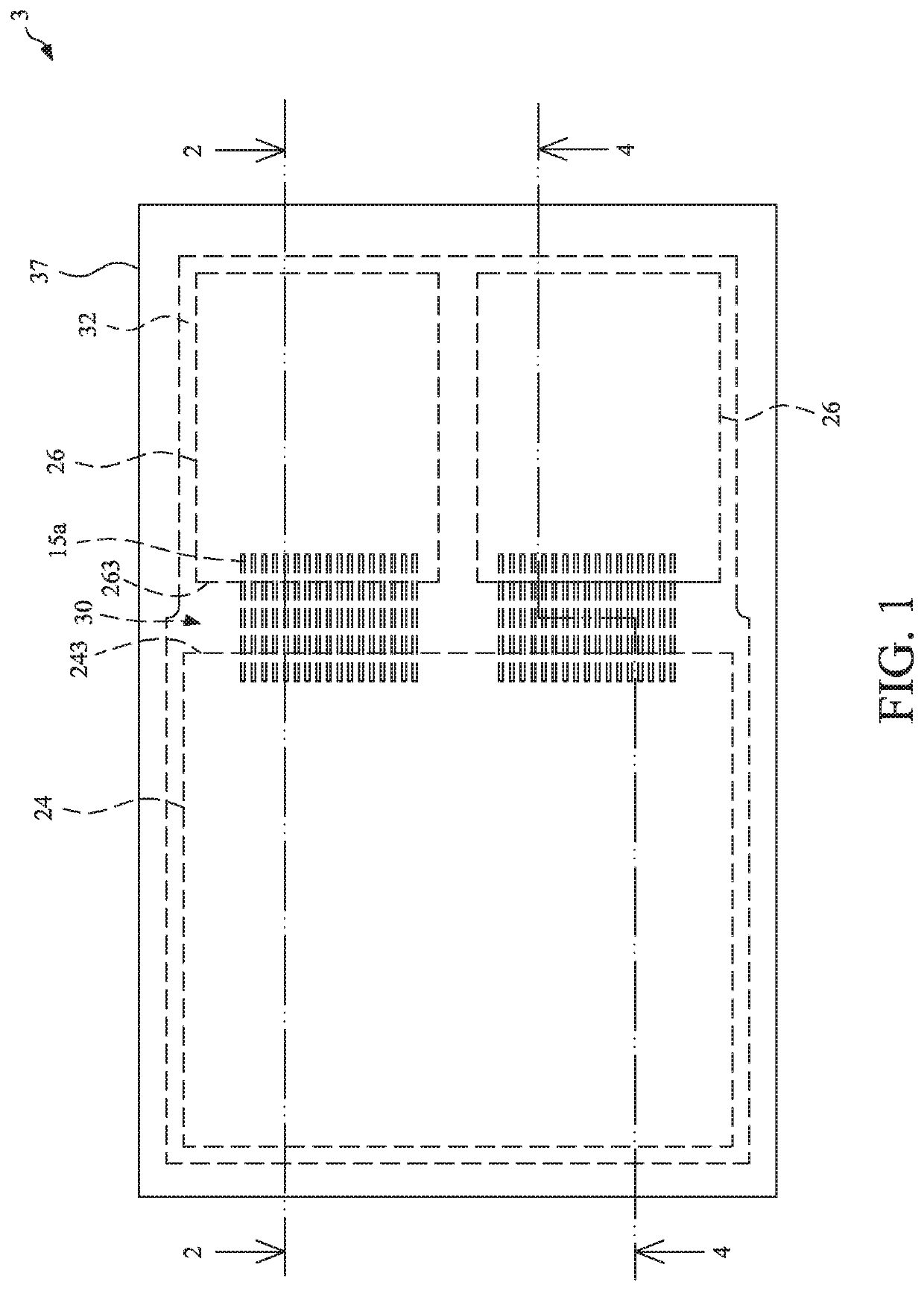
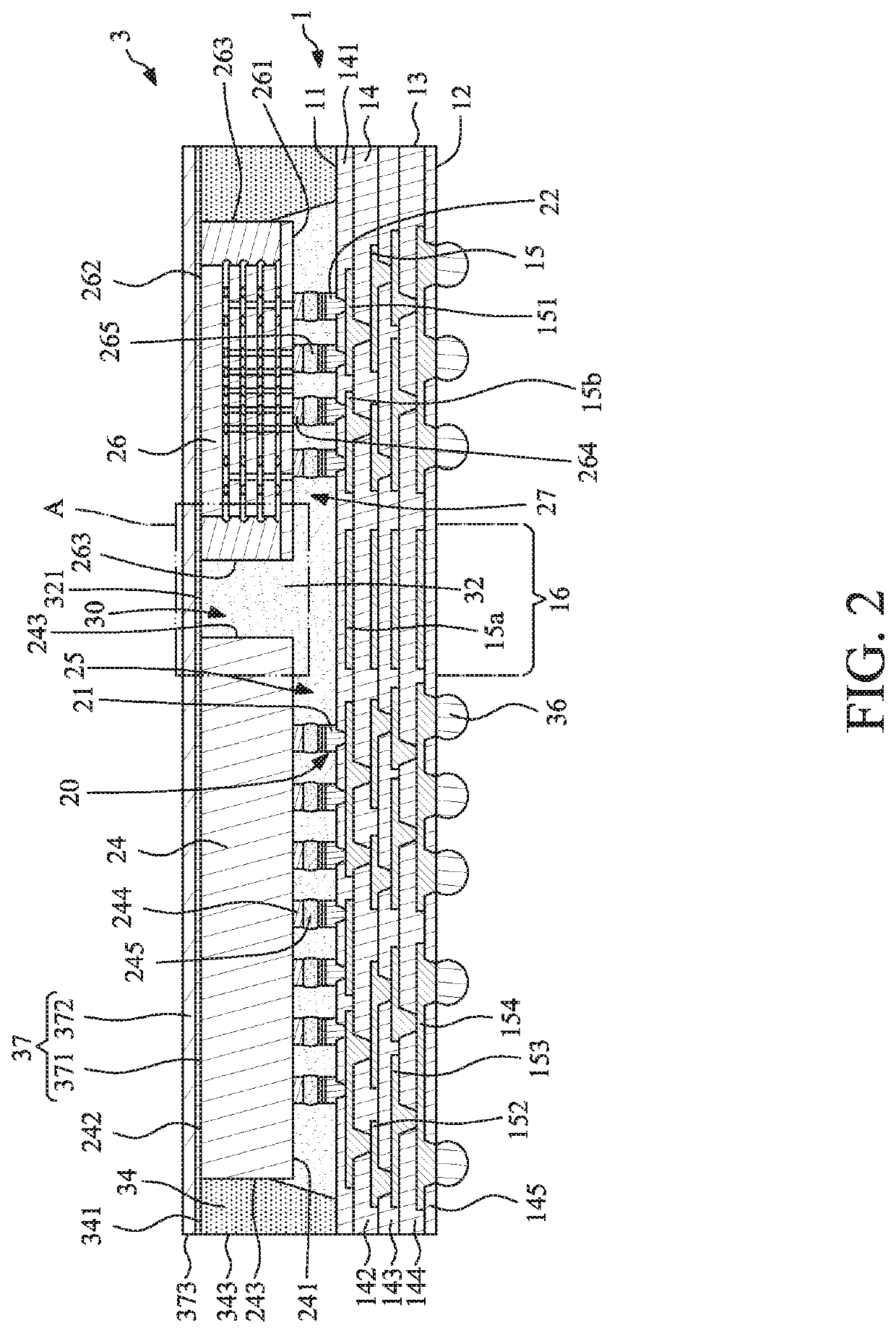
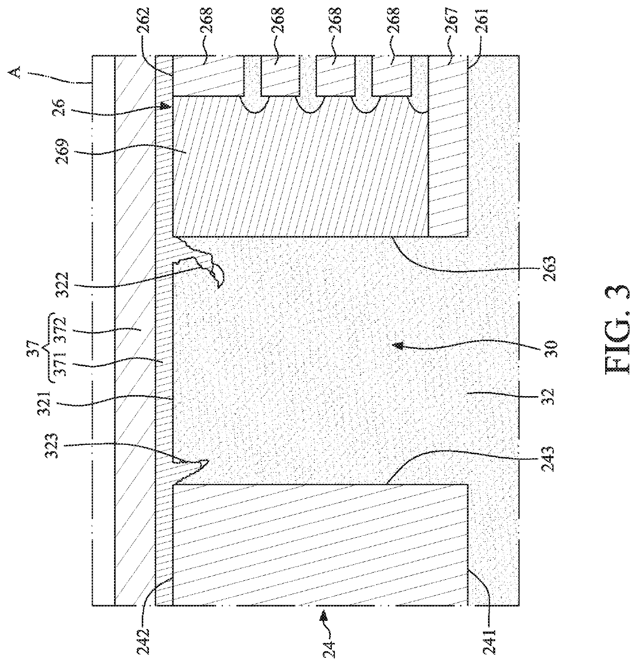
[0059]Common reference numerals are used throughout the drawings and the detailed description to indicate the same or similar components. Embodiments of the present disclosure will be readily understood from the following detailed description taken in conjunction with the accompanying drawings.

[0060]The following disclosure provides many different embodiments, or examples, for implementing different features of the provided subject matter. Specific examples of components and arrangements are described below to explain certain aspects of the present disclosure. These are, of course, merely examples and are not intended to be limiting. For example, the formation of a first feature over or on a second feature in the description that follows may include embodiments in which the first and second features are formed or disposed in direct contact, and may also include embodiments in which additional features may be formed or disposed between the first and second features, such that the fir...


PUM


Abstract

A package structure includes a wiring structure, a first electronic device, a second electronic device, a protection material and a reinforcement structure. The first electronic device and the second electronic device are electrically connected to the wiring structure. The protection material is disposed between the first electronic device and the wiring structure and between the second electronic device and the wiring structure. The reinforcement structure is disposed on and contacts the first electronic device and the second electronic device. The reinforcement structure contacts the protection material.

Description

BACKGROUND1. Field of the Disclosure[0001]The present disclosure relates to a package structure and a manufacturing method, and to a package structure including a reinforcement structure, and a method for manufacturing the same.2. Description of the Related Art[0002]In a semiconductor assembly structure, a semiconductor package structure is mounted to a substrate, and a heat sink is attached to a top surface of the semiconductor package structure so as to dissipate the heat generated from the semiconductor device(s) in the semiconductor package during operation. However, when the heat sink is attached to the semiconductor package structure, a pressing force may be transmitted from the heat sink to the semiconductor package structure. Since a rigidity or stiffness of the semiconductor package structure is relatively low, a crack may be formed at the top surface of the semiconductor package structure. In addition, during a manufacturing process, several thermal process (e.g., reflow p...

Claims


Application Information

Patent Timeline
Patent Type & Authority Applications(United States)
IPC IPC(8): H01L23/00H01L25/065H01L23/31H01L25/00H01L21/56
CPCH01L23/562H01L25/0652H01L21/56H01L25/50H01L23/3135H01L23/3128H01L23/16H01L23/367H01L23/3736H01L25/16H01L21/568H01L21/563H01L21/6835H01L2221/68345H01L2221/6834H01L2221/68327H01L25/18H01L25/03H01L23/36H01L23/49816H01L23/5383H01L23/5389H01L23/3675H01L23/14H01L23/42H01L2224/73204H01L2224/16225H01L2224/32225H01L2924/15311H01L2924/00
Inventor FANG, HSU-NANYEH, YUNG-I
Owner ADVANCED SEMICON ENG INC
Learn More