Package for installing semiconductor element, and semiconductor device

a technology for semiconductor elements and packages, applied in semiconductor devices, semiconductor/solid-state device details, electrical devices, etc., can solve the problems of inability to achieve a long-life, high-power, and highly reliable package for installing semiconductor elements, and achieve the effects of long-life, high-power, and high-reliability

Pending Publication Date: 2021-06-10
PANASONIC HLDG CORP
View PDF0 Cites 0 Cited by
  • Summary
  • Abstract
  • Description
  • Claims
  • Application Information

AI Technical Summary

Benefits of technology

[0016]Specifically, airtightness within the package for installing a semiconductor element can be secured by joining the flange placed on the top surface of the ceramic frame with a planar glass or a glass lens by Au / Sn sealing / bonding. In addition, since the metal reflector fitted in the housing portion of the ceramic frame covers further on the top surface of the ceramic frame that is irradiated with light, and it is easy to change the opening area on the side in which the opening area is small, optical design freedom is provided. Further, since the metal reflector is plated as optimal for a wavelength emitted from the semiconductor element, the light extraction efficiency is satisfactory. Therefore, the configuration makes it possible to provide a long-life, high-power, and highly reliable package for installing a semiconductor element.
[0017]The present disclosure can provide a long-life, high-power, and highly reliable package for installing a semiconductor element.

Problems solved by technology

However, a problem with the configuration disclosed in Japanese Unexamined Patent Application Publication No. 2008-47916 is that it is difficult to secure airtightness because there is much less area for adhesive application on the planar glass or the glass lens due to the package construction.
Consequently, the inner area of ring 134 is constrained, which leads to another problem of being unable to secure sufficient reflection of light emitted from a light-emitting element.
Accordingly, a problem with the configuration disclosed in Japanese Unexamined Patent Application Publication No. 2008-47916 is that it is not possible to achieve a long-life, high-power, and highly reliable package for installing a semiconductor element.

Method used


Image

  • Package for installing semiconductor element, and semiconductor device
  • Package for installing semiconductor element, and semiconductor device
  • Package for installing semiconductor element, and semiconductor device

Examples


example 1

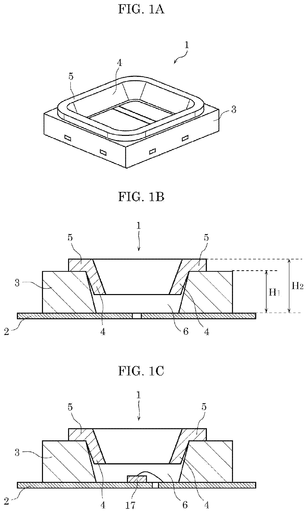
[0035]FIGS. 1A to 1C illustrate package 1 for installing a semiconductor element of Example 1 according to the present disclosure. FIG. 1A is a perspective view of package 1 for installing a semiconductor element of Example 1 according to the present disclosure. FIG. 1B is a sectional view of package 1 for installing a semiconductor element of Example 1 according to the present disclosure. FIG. 1C is a sectional view of a semiconductor device of Example 1 according to the present disclosure. Now that the overall picture of package 1 for installing a semiconductor element of Example 1 is grasped with reference to FIG. 1A, description will now be made with reference to the sectional view in FIG. 1B.

[0036]As illustrated in FIG. 1B, package 1 for installing a semiconductor element of Example 1 includes lead frame 2, resin frame 3 including housing portion 6, and metal reflector 4 including flange 5. Resin frame 3 is a specific example of a frame. More specifically, package 1 for install...

example 2

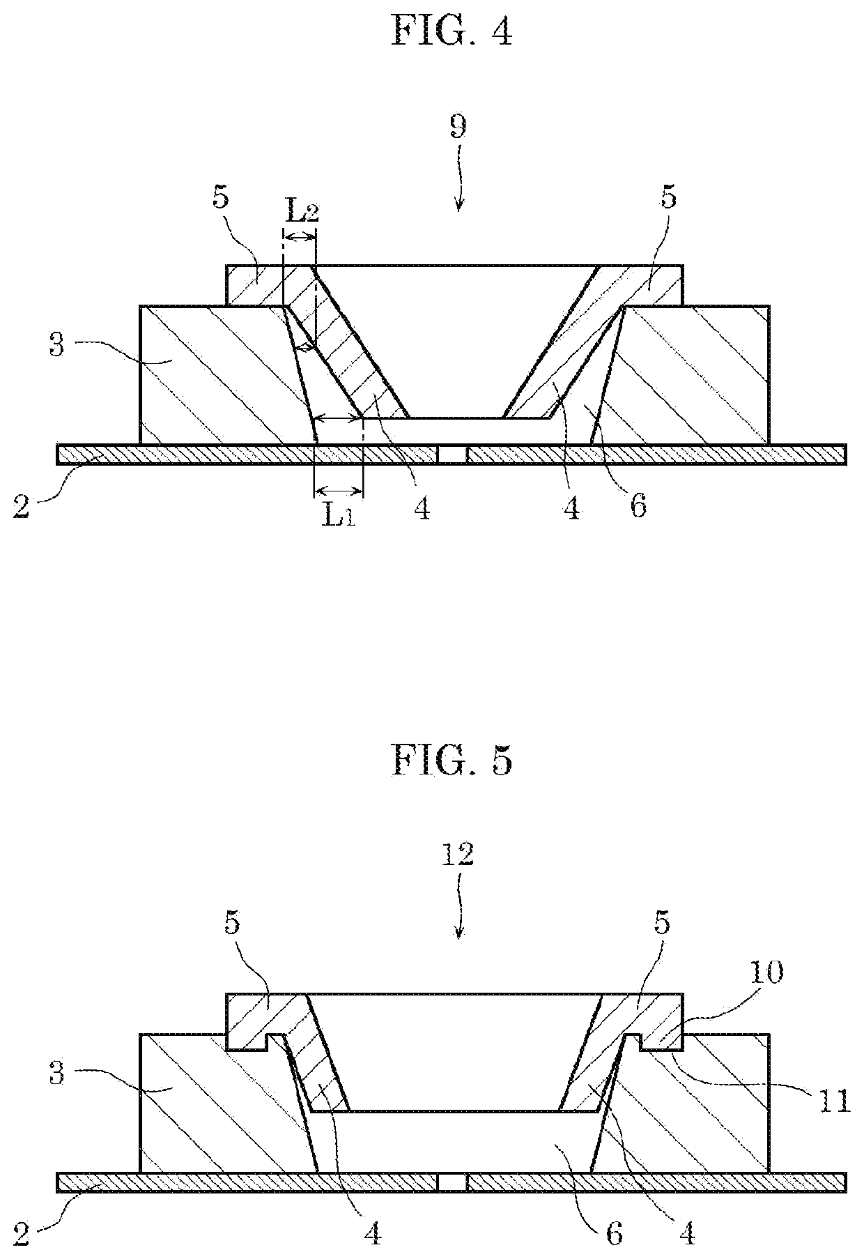
[0052]In Example 2 below, differences from Example 1 will mainly be described with reference to FIG. 4.

[0053]FIG. 4 is a sectional view of package 9 for installing a semiconductor element of Example 2 according to the present disclosure. Like elements as those in other figures such as FIG. 1B are given the same reference characters, and detailed description thereof will not be repeated.

[0054]As in Example 1, package 9 for installing a semiconductor element of Example 2 includes: lead frame 2; resin frame 3 disposed on lead frame 2 and including housing portion 6 formed by an opening that widens with the distance in the upward direction from lead frame 2; and metal reflector 4 that fits in housing portion 6 and includes an opening portion corresponding to housing portion 6 of resin frame 3. The opening area of the opening portion of metal reflector 4 increases with the distance in the upward direction from lead frame 2, and metal reflector 4 includes flange 5 around the side of metal...

example 3

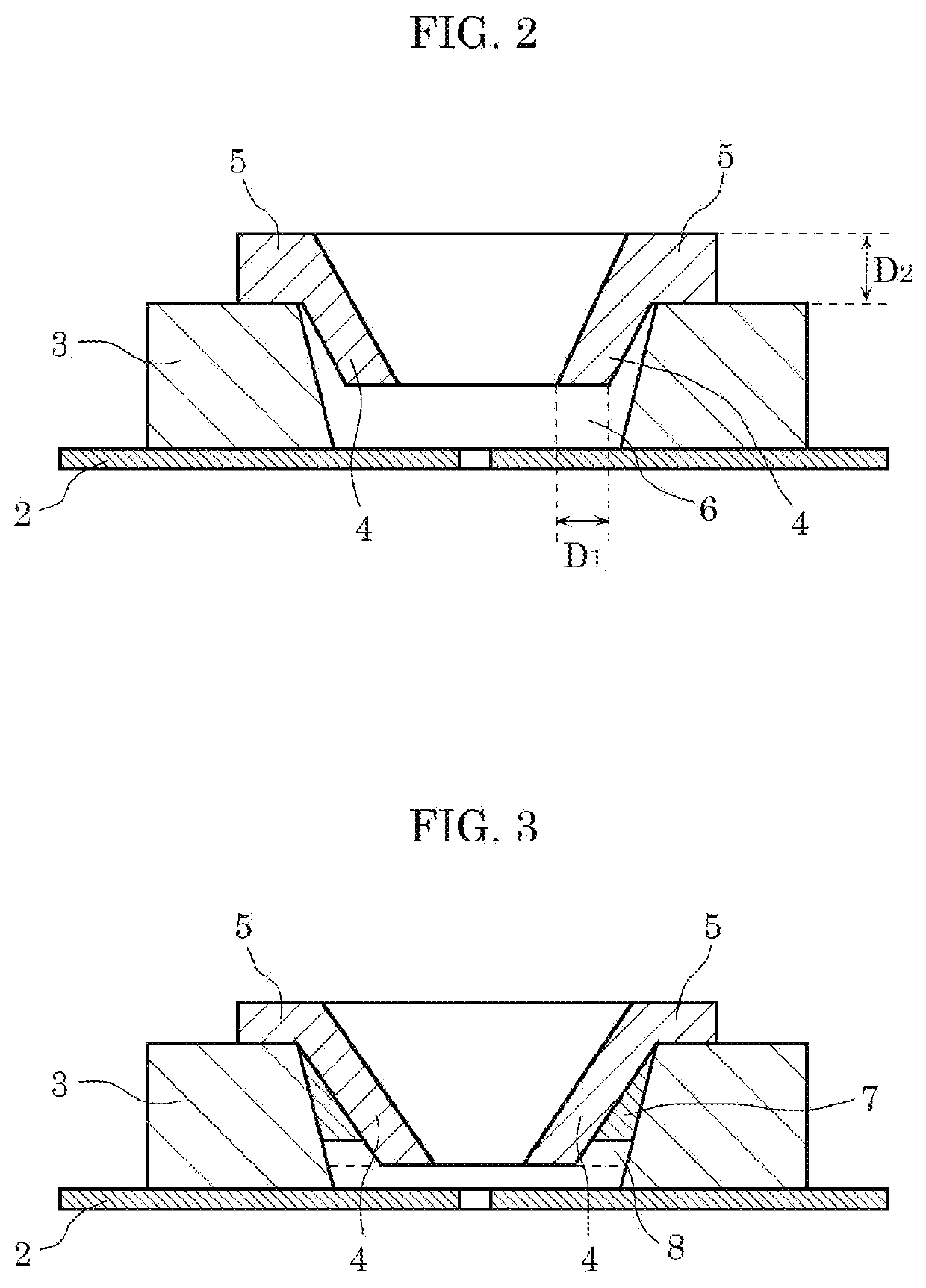
[0058]In Example 3 below, a bonding method of metal reflector 4 different from Example 1 and Example 2 will be described with reference to FIG. 1B.

[0059]As in Example 1, package 1 for installing a semiconductor element of Example 3 includes: lead frame 2; resin frame 3 disposed on lead frame 2 and including housing portion 6 formed by an opening that widens with the distance in the upward direction from lead frame 2; and metal reflector 4 that fits in housing portion 6 and includes an opening portion corresponding to housing portion 6 of resin frame 3. The opening area of the opening portion of metal reflector 4 increases with the distance in the upward direction from lead frame 2, and metal reflector 4 includes flange 5 around the side of metal reflector 4 in which the opening area is large, and flange 5 is placed on the top surface of resin frame 3.

[0060]Furthermore, in package 1 for installing a semiconductor element of Example 3, resin frame 3 and metal reflector 4 are in direct...


PUM

PropertyMeasurementUnit
thicknessaaaaaaaaaa
thicknessaaaaaaaaaa
thicknessaaaaaaaaaa

Abstract

A package for installing a semiconductor element includes: a lead frame; a resin frame disposed on the lead frame and including a housing portion formed by an opening that widens with the distance in the upward direction from the lead frame; and a metal reflector that fits in the housing portion and includes an opening portion corresponding to the housing portion of the resin frame. The opening area of the opening portion of the metal reflector increases with the distance in the upward direction from the lead frame, and the metal reflector includes a flange around the side of the metal reflector in which the opening area is large. The flange is placed on the top surface of the resin frame.

Description

CROSS REFERENCE TO RELATED APPLICATIONS[0001]This application is a U.S. continuation application of PCT International Patent Application Number PCT / JP2019 / 034036 filed on Aug. 30, 2019, claiming the benefit of priority of Japanese Patent Application Number 2018-163252 filed on Aug. 31, 2018, the entire contents of which are hereby incorporated by reference.BACKGROUND1. Technical Field[0002]The present disclosure relates to an LED package, and in particular to a high-power and highly reliable LED package that is excellent in airtightness and heat dissipation, is corrosion resistant, and has high light extraction efficiency.2. Description of the Related Art[0003]Along with development of blue LED chips, for LED packages, there has been a need for phosphor-converted white LED packages. In addition, LED packages have ranged from those packages for small backlights of televisions, smartphones, cameras, in-vehicle instrument panels, and the like to large and high-power LED packages for LE...

Claims


Application Information

Patent Timeline
Patent Type & Authority Applications(United States)
IPC IPC(8): H01L33/60H01L33/48H01L33/62
CPCH01L33/60H01L33/62H01L33/486H01L33/644H01L23/29H01L23/31
Inventor NIWA, IKUOHASE, YASUTAKAAKAI, SHUNSUKETAKAGI, HAYATOYOKOTA, TOMOYUKISANADA, HIROSHI
Owner PANASONIC HLDG CORP
Why Eureka
Try Eureka