Laser reflow apparatus and laser reflow method

a laser reflow and laser reflow technology, which is applied in the direction of soldering apparatus, instruments, manufacturing tools, etc., can solve the problems of substrate warpage, connection failure, and concern for wafer warpage in wafer-on, and achieve high laser power, prevent pump connection failure, and reliably melt solder bumps

Pending Publication Date: 2021-07-01
DISCO CORP
View PDF4 Cites 2 Cited by
  • Summary
  • Abstract
  • Description
  • Claims
  • Application Information

AI Technical Summary

Benefits of technology

[0019]According to the aspect and the other aspect of the present invention, since the laser reflow apparatus incorporates the spatial beam modulation unit, it is capable of setting a laser power density locally in the irradiation range. For example, a laser beam having a high laser power can be applied to only solder bump areas to reliably melt solder bumps while restraining the workpiece from warping by not wastefully heating unnecessary areas, thereby preventing pump connection failures.

Problems solved by technology

Though the laser reflow process has advantages of its own as described above, it still suffers a substrate warpage problem because the board is heated by the laser beam applied thereto, and hence remains to be improved further.
However, the reduced output power of the laser might not sufficiently melt the solder bumps, possibly resulting in connection failures.
However, there is still concern for wafer warpage in wafer-on-wafer applications.

Method used


Image

  • Laser reflow apparatus and laser reflow method
  • Laser reflow apparatus and laser reflow method
  • Laser reflow apparatus and laser reflow method

Examples


Embodiment Construction

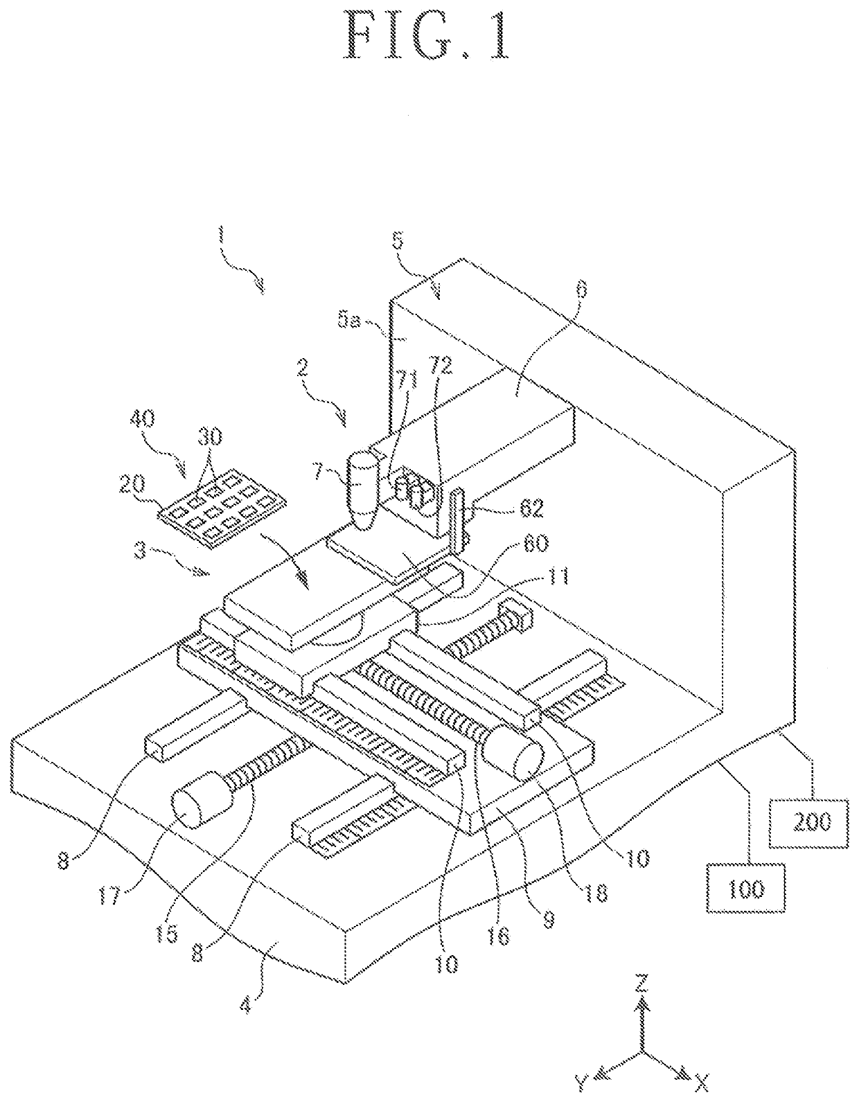
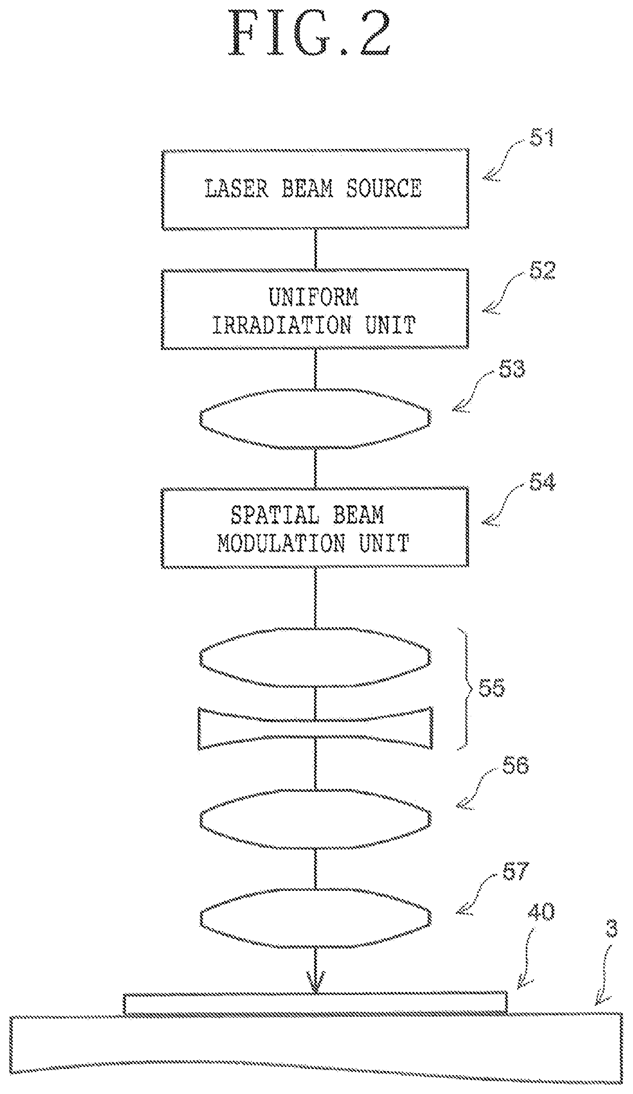
[0040]A laser reflow apparatus according to an embodiment of the present invention will be described below with reference to the accompanying drawings. As illustrated in FIG. 1, the laser reflow apparatus 1 includes a laser beam applying unit 2 for applying a laser beam to a workpiece 40 and a processing table 3 for holding the workpiece 40 thereon. The laser reflow apparatus 1 processes the workpiece 40 held on the processing table 3 with the laser beam by moving the processing table 3 relatively to the laser beam applying unit 2.

[0041]The workpiece 40 includes a rectangular board 20 on which an array of semiconductor chips 30 is disposed with their face sides facing downwardly. The semiconductor chips 30 are mounted on the board 20 according to a flip-chip packaging process by reflowing solder bumps on the face sides of the semiconductor chips 30 with a laser beam. The board 20 may be a printed-circuit board (PCB), a device wafer prior to being divided into chips, or the like, for...


PUM

PropertyMeasurementUnit
wavelengthaaaaaaaaaa
densityaaaaaaaaaa

Abstract

A laser reflow apparatus reflows solder bumps disposed on a side of a semiconductor chip in a workpiece and included in an irradiation range on the workpiece by applying a laser beam to an opposite side of the semiconductor chip. The laser reflow apparatus includes a spatial beam modulation unit including a laser power density setting function to locally set the laser power density in the irradiation range of a laser beam emitted from a laser beam source, and an image focusing unit including an image focusing function to focus the laser beam emitted from the laser beam source and apply the focused laser beam to the irradiation range on the workpiece.

Description

BACKGROUND OF THE INVENTIONField of the Invention[0001]The present invention relates to a laser reflow apparatus and a laser reflow method for reflowing solder bumps by which a semiconductor chip is connected to a board in a workpiece by applying a laser beam to the workpiece through the semiconductor chip.Description of the Related Art[0002]Heretofore, there has been known a flip-chip packaging technology in which a semiconductor chip having solder bumps is flipped over and placed on a board with the solder bumps interposed therebetween and the entire assembly of the board and the chip is heated to melt the solder bump to connect to electrodes on the board.[0003]The flip-chip packaging technology includes a known mass reflow process for heating a board in its entirety for bonding semiconductor chips to the board. According to the mass reflow process, there is known the possibility that while the board is being heated, the board may be warped to a large extent due to the difference ...

Claims


Application Information

Patent Timeline
Patent Type & Authority Applications(United States)
IPC IPC(8): H01L23/00G02B19/00B23K26/06B23K26/03B23K1/005B23K1/00B23K3/08
CPCH01L24/75B23K2101/40G02B19/0047G02B19/0009B23K26/0608B23K26/0665B23K26/034B23K26/0648B23K1/0056B23K1/0016B23K3/08H01L2924/3511H01L2224/75253H01L2224/75263H01L2224/7555H01L2224/81224H01L2224/81815H01L24/81B23K2101/42B23K26/067B23K26/0853B23K26/032B23K26/037B23K26/082H01L2224/16225H01L2224/13101H01L2224/75901H01L2924/15311H01L24/16H01L24/13H01L2224/16145H01L2224/7598H01L2224/753H01L25/50H01L2224/17135H01L2224/14135H01L24/14H01L24/17H01L2225/06517H01L2225/06513H01L2224/17181H01L25/0652H01L25/18H01L25/0655G02B27/30G02B27/0944G02B27/0955H01L2924/014H01L2924/00014B23K26/073H05K3/34
Inventor KOBAYASHI, SATOSHIKIM, YOUNGSUKKIMURA, NOBUYUKIIKKU, YUKICHEN, ZHIWEN
Owner DISCO CORP
Why Eureka
Try Eureka