Method of manufacturing an electronic component

a manufacturing method and electronic component technology, applied in the direction of manufacturing tools, welding/cutting media/materials, manufacturing tools, etc., can solve the problems of difficult to remove voids from solder, difficult to reduce the number of voids, and inability to withstand high temperature, so as to reduce the voids in the solder and reliably melt the solder

Inactive Publication Date: 2007-10-04
NEC ELECTRONICS CORP
View PDF5 Cites 4 Cited by
  • Summary
  • Abstract
  • Description
  • Claims
  • Application Information

AI Technical Summary

Benefits of technology

[0032] According to the invention, the first heating temperature of the first heating is lower than the second heating temperature of the second heating in the vaporizing the solvent and the resin component in the solder. Therefore, in the first heating, since the solvent is sufficiently contained in the solder, the activator can sufficiently function, and the oxide film formed on the solder surface can be reliably removed. In this manner, the third heating process is performed, and the solder can be reliably melted in the third heating in which the solder is melted.
[0033] Furthermore, since the solder is kept at the first heating temperature for the predetermined period of time, the oxide film formed on the solder surface can be more reliably removed.
[0034] In the present invention, the second heating process is performed to vaporize the solvent and the resin component. For this reason, in the performing the third heating process and melting the solder, the solvent and the resin component rarely vaporized. Thus, the number of voids which are generated in the solder can be sufficiently reduced.
[0035] Furthermore, in the present invention, since the solder is kept at the second heating temperature for the predetermined period of time, the solvent and the resin component can be more reliably vaporized.
[0039] According to the present invention, there is provided to a method of manufacturing an electronic component which can reduce voids in the solder to make it possible to reliably melt the solder.

Problems solved by technology

Thus, there is a possibility that the members constituting the electronic component cannot withstand the high temperature and may be deteriorated.
For this reason, in the technique in Japanese Laid-open patent publication No. 2004-6682, it is considered that it is difficult to remove the voids from the solder.
Therefore, the number of voids is difficult to be reduced.

Method used


Image

  • Method of manufacturing an electronic component
  • Method of manufacturing an electronic component
  • Method of manufacturing an electronic component

Examples


example

[0100] An example of the present invention will be described below.

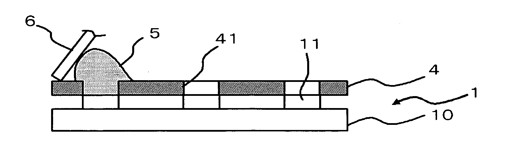
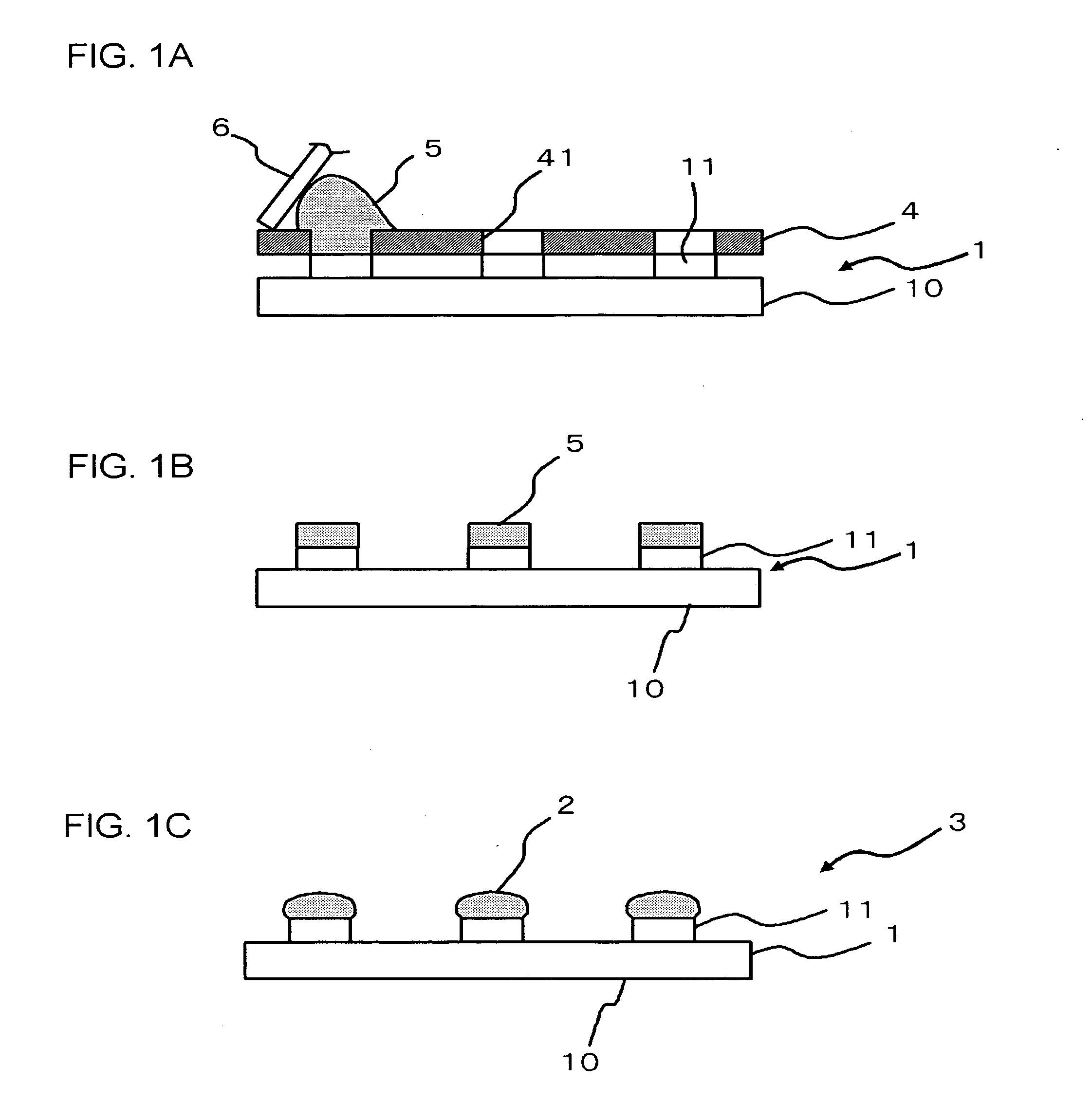
[0101] As in the above embodiment, a substrate which comprises a base material which is a silicon wafer and electrodes formed on the base material was prepared.

[0102] A solder was printed on the electrodes of the substrate by the same method as that in the embodiment.

[0103] As the solder, a solder containing a solvent (organic solvent), a resin component (rosin), an activator (organic amine hydrochloride), a thixotropic agent, and a brazing filler metal (95% lead by weight and 5% tin by weight) was used.

[0104] As in the above embodiment, the solder was heated to form a solder bump.

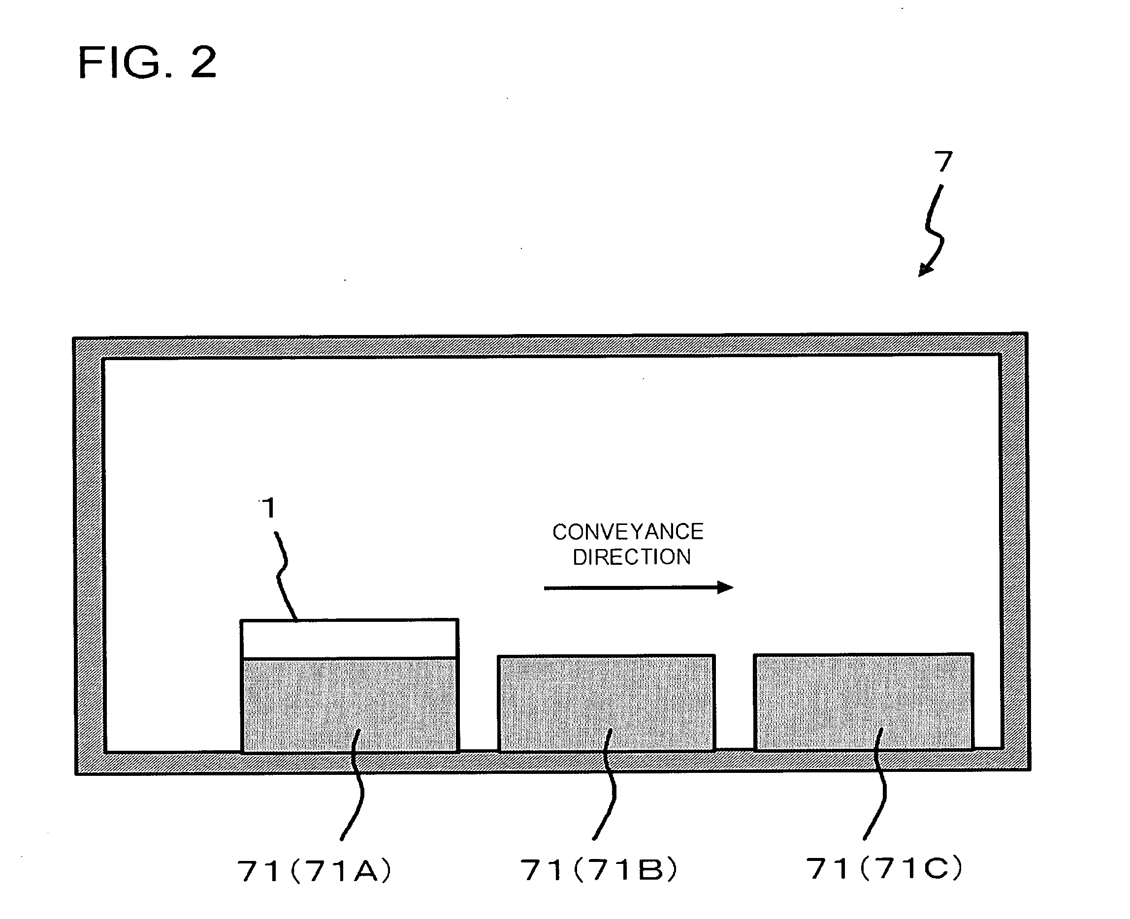
[0105] In this case, a first heating temperature for the solder was set at 140oC to 170oC. The first heating temperature was kept for 30 seconds to 120 seconds.

[0106] A second heating temperature for the solder was set at 290oC or more and lower than the melting point of the solder. The solder was kept at the second heating temperatur...


PUM

PropertyMeasurementUnit
temperatureaaaaaaaaaa
melting pointaaaaaaaaaa
concentrationaaaaaaaaaa

Abstract

A method of manufacturing an electronic component which can reduce voids in a solder and can reliably melt the solder is provided. The method of manufacturing an electronic component including a member (substrate 1) having a metal junction (electrode 11) includes: the step of supplying a solder 5 containing a solvent, a resin component, an activator, and a brazing filler metal to the junction (electrode 11); the first heating step in which a first heating process to the solder 5 is performed and the solder 5 is kept at a first heating temperature for a predetermined period of time; the second heating step in which a second heating process to the solder 5 is preformed and the solder 5 is kept at a second heating temperature higher than the first heating temperature for a predetermined period of time to vaporize the solvent and the resin component; and the third heating step in which a third heating process to the solder 5 is performed and the solder 5 is melted.

Description

[0001] This application is based on Japanese Patent application NO. 2005-298789, the content of which is incorporated hereinto by reference. BACKGROUND [0002] 1. Technical Field [0003] The present invention relates to a method of manufacturing an electronic component. [0004] 2. Related Art [0005] Solder is conventionally used in connection between members which constitute an electronic component. [0006] For example, a first member and a second member constituting an electronic component are jointed to each other with a solder as described below. [0007] A solder (conductive paste) is supplied onto a joint surface of the first member which constitutes the electronic component, and the second member which constitutes the electronic component is placed on the first member. Thereafter, the first member and the second member are preheated for a predetermined period of time at a temperature at which the solder does not melt. [0008] The preheating is performed to uniform the temperatures of...

Claims


Application Information

Patent Timeline
Patent Type & Authority Applications(United States)
IPC IPC(8): B23K31/02
CPCB23K3/0692B23K2201/40H05K3/3484H01L24/11H05K2203/043H05K2203/1476H05K3/3494B23K2101/40H01L2224/05568H01L2224/05573H01L2924/00014H05K3/3485H01L2224/05599
Inventor INOMATA, TERUJISUGIURA, MASATOSHI
Owner NEC ELECTRONICS CORP
Why Eureka
Try Eureka