Power semi-conductor module, mask, measurement method, computer software, and recording medium

Pending Publication Date: 2021-07-22
MITSUBISHI ELECTRIC CORP
View PDF0 Cites 0 Cited by
  • Summary
  • Abstract
  • Description
  • Claims
  • Application Information

AI Technical Summary

Benefits of technology

[0005]The invention i

Problems solved by technology

To fix a sensor on it is difficult,

Method used


Image

  • Power semi-conductor module, mask, measurement method, computer software, and recording medium
  • Power semi-conductor module, mask, measurement method, computer software, and recording medium
  • Power semi-conductor module, mask, measurement method, computer software, and recording medium

Examples


Example

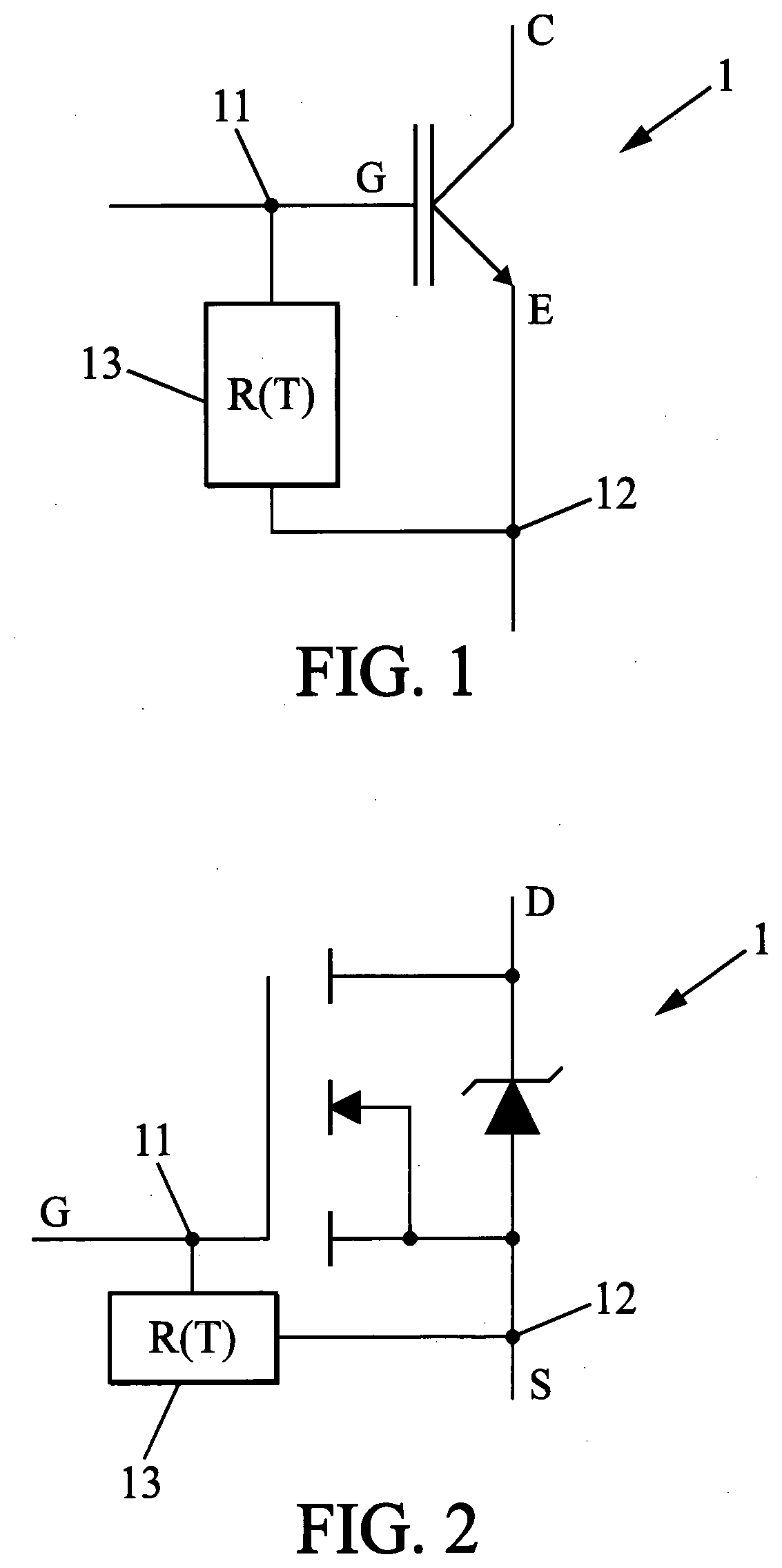
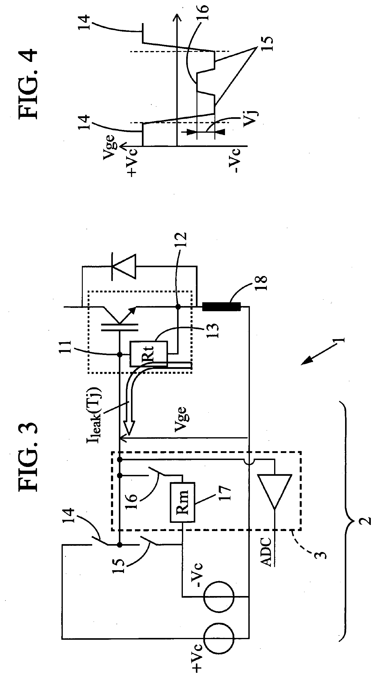
[0081]It is now referred to FIG. 8 and FIG. 9. In such a first embodiment, the thermistor is formed by creating a polysilicon link between at least a first electrode trench 2111 and an N+ doping region corresponding to an active area of the semi-conductor material. As it can be seen on FIG. 8, the internal wall of each one of the three dummy trenches 2112 is coated with an isolating film 123, an oxide similar to the oxide of the oxide layer 107 in the example. In such a way, the interior of the trench is electrically isolated from the rest of the superposition 100. Each one of the three dummy trenches 2112 are filled, inside the isolating film 123, with polysilicon filling 121. The polysilicon 121 enables to conduct electricity along the dummy trench 2112 (in the horizontal direction of FIG. 7). The first electrode trench 2111 is coated with an isolating film 133, an oxide similar to the oxide of the oxide layer 107 in the example. In such a way, the interior of the trench is electr...

Example

[0096]It is now referred to FIG. 10 and FIG. 11. In such a second embodiment, the thermistor is formed by creating a polysilicon link between at least a dummy trench 2112 and a first electrode trench 2111. The second embodiment is easier to implement than the first embodiment.

[0097]On FIG. 10 and FIG. 11, elements similar to these of the preceding figures have the same numerical references. By comparison to the first embodiment (FIG. 8 and FIG. 9), the plugs are absent. Plugs 144 are provided on top of the dummy trenches 2112 through the BPSG layer 108. The most part of the oxide layer 107 of the superposition 100 is replaced by a polysilicon layer 120 on top of the dummy trenches 2112. The polysilicon layer 120 covers at least the top of the dummy trenches 2112.

[0098]Usually, and as it is represented on FIG. 10, the electric isolation between the polysilicon filling 121 in the dummy trenches 2112 and the polysilicon filling 131 in the first electrode trench 2111 is ensured by a por...

Example

[0111]In such a third embodiment, the thermistor is formed by extension of at least one dummy trench 2112 until the first electrode 11 (the gate line). Thus the Emitter / Collector potential reaches and touches a line of the Gate potential. In various embodiments, the line pattern may also be modified to facilitate the connection to the extended trench.

[0112]As it can be seen on FIG. 12, the polysilicon filling 121 in a dummy trench 2112 and the polysilicon layer 161 of the first electrode part are usually separated on from the other. In addition, each one is surrounded by an isolating film 123 (oxide layer), respectively 163, in order to electrically isolate them from the environment. By comparison, as it can be seen on FIG. 13 of the third embodiment, an extension part of polysilicon material is provided between the polysilicon filling 121 of the dummy trench 2112 and the polysilicon layer 161 of the first electrode part. In the third embodiment, the said extension part forms the mo...


PUM


Abstract

Power semi-conductor module (1) comprising: —at least one IGBT with a Gate G forming a first electrode (11) and an Emitter E forming a second electrode (12), or—at least one MOSFET with a Gate G forming a first electrode (11) and a Source S forming a second electrode (12). The first electrode (11) includes a polysilicon material made in one piece. The one-piece is made partly of a monitoring portion (13). The monitoring portion (13) is in electrical contact with the second electrode (12) such that a leakage current flows between the first electrode (11) and the second electrode (12) in an operational state of the module (1). The monitoring portion (13) has a location, a form, a size and a material composition selected together such that to have a variable resistance in function of its temperature during the operational state of the module (1).

Description

TECHNICAL FIELD[0001]The invention pertains to the technical field of power semiconductor devices. More specifically, the invention is related to the monitoring of such devices.BACKGROUND ART[0002]Monitoring temperatures in power semi-conductor devices, like Insulated Gate Bipolar Transistors (IGBTs) and Metal-Oxide-Semiconductor Field-Effect Transistors (MOSFETs) is an important function. For example, it is useful for protection, condition and health monitoring. It is known to add specific sensors as close as possible to the die, the die being generally the most important and the hottest part of such devices. The temperature can be measured directly by using temperature sensors, or indirectly by using other sensors.[0003]Generally, the free surface of a die is very small. To fix a sensor on it is difficult, and even impossible in some cases. To circumvent this problem, it is usual to dispose the sensor at a distance from the die and to use mathematical function to correct and deduc...

Claims


Application Information

Patent Timeline
IPC IPC(8): G01R31/26H01L29/739H01L29/78H01L23/34
CPCG01R31/2644H01L29/7397H01L29/7813G01R31/275G01R31/2642H01L23/34H01L29/7803H03K17/0812H03K2017/0806
Inventor DEGRENNE, NICOLAS
Owner MITSUBISHI ELECTRIC CORP
Why Eureka
Try Eureka