Wafer probe station

a probe station and probe technology, applied in the field of wafer probe stations, can solve problems such as electronic device components, and achieve the effect of accurate and easy to obtain the actual change of operation

Active Publication Date: 2021-10-28
MICROELECTRONICS TECH INC
View PDF0 Cites 0 Cited by
  • Summary
  • Abstract
  • Description
  • Claims
  • Application Information

AI Technical Summary

Benefits of technology

[0004]A technical aspect of the present disclosure is to provide a wafer probe station, which can accurately and easily obtain the actual change of the operation distance between the probes and the device under test in a vertical direction after a temperature change of the thermal chuck to the operational temperature.

Problems solved by technology

As the demand for electronic devices has been increasing nowadays, the quality of the components of the electronic devices correspondingly becomes an important issue of the semiconductor industry.

Method used


Image

  • Wafer probe station
  • Wafer probe station

Examples


Embodiment Construction

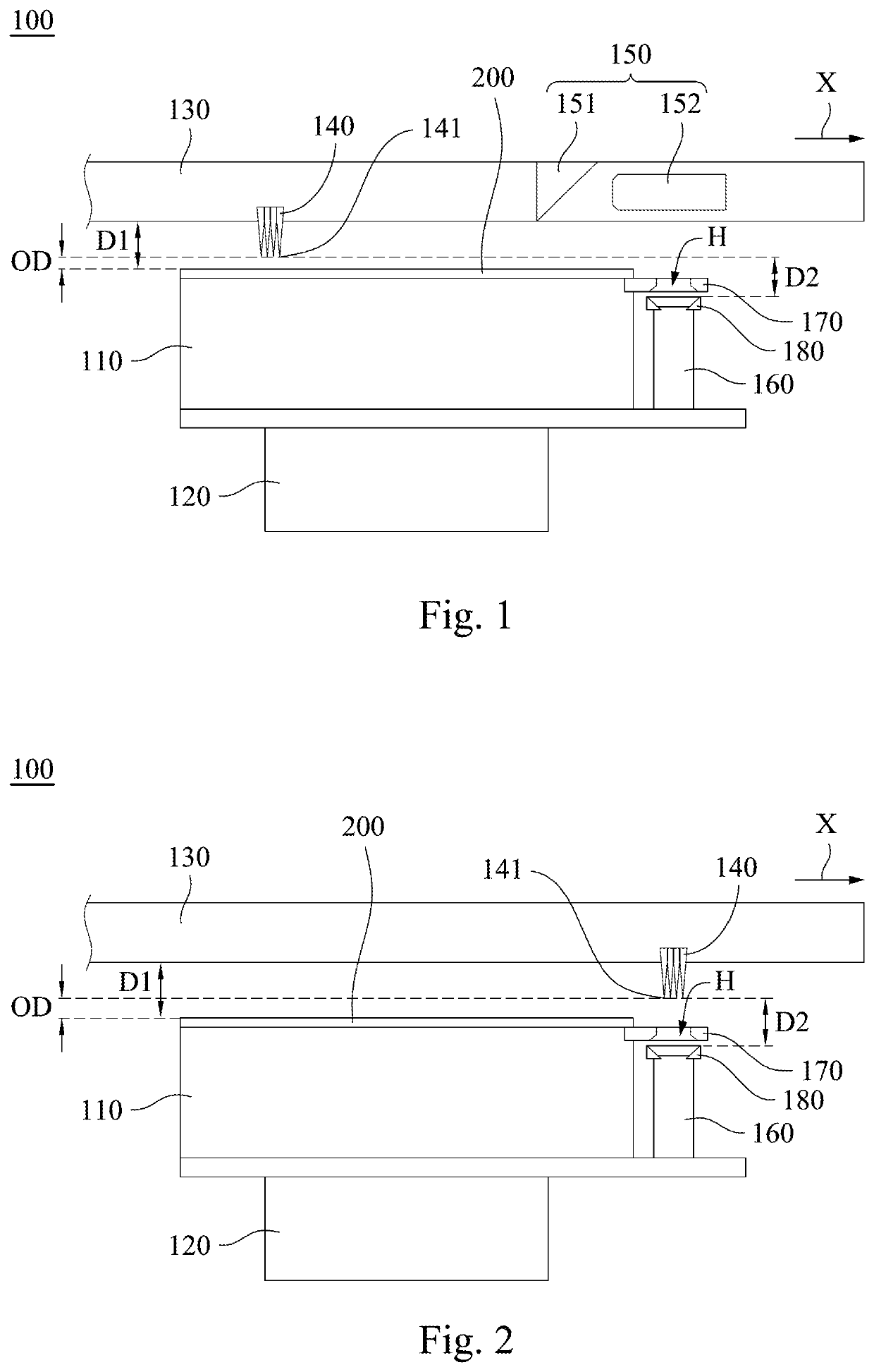
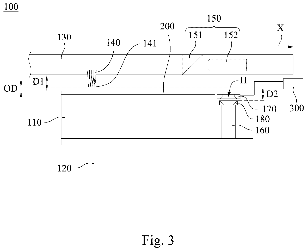
[0024]Drawings will be used below to disclose embodiments of the present disclosure. For the sake of clear illustration, many practical details will be explained together in the description below. However, it is appreciated that the practical details should not be used to limit the claimed scope. In other words, in some embodiments of the present disclosure, the practical details are not essential. Moreover, for the sake of drawing simplification, some customary structures and elements in the drawings will be schematically shown in a simplified way. Wherever possible, the same reference numbers are used in the drawings and the description to refer to the same or like parts.

[0025]Unless otherwise defined, all terms (including technical and scientific terms) used herein have the same meanings as commonly understood by one of ordinary skill in the art to which this disclosure belongs. It will be further understood that terms, such as those defined in commonly used dictionaries, should ...


PUM


Abstract

A wafer probe station includes a thermal chuck, a chuck stage, a platen, some probes, a first focusing device, a second focusing device and a thermal plate. The thermal chuck heats up to an operational temperature and holds a device under test (DUT). The chuck stage connects with the thermal chuck and moves the thermal chuck. The thermal chuck locates between the chuck stage and the platen. The probes are disposed on the platen and configured to contact with the DUT. The first focusing device is disposed on the platen to focus on the DUT. The second focusing device is disposed on the chuck stage to focus on the probes. The thermal plate locates between the second focusing device and the platen and is configured to heat up to the operational temperature. The thermal plate has a through hole aligning with the second focusing device.

Description

BACKGROUNDTechnical Field[0001]The present disclosure relates to wafer probe stations.Description of Related Art[0002]As the demand for electronic devices has been increasing nowadays, the quality of the components of the electronic devices correspondingly becomes an important issue of the semiconductor industry. Apart from the improving technology of manufacture for the components, the accuracy of testing for the components has also become more important.[0003]For example, wafer probe stations are in general used to test the quality of the wafers or dies in the semiconductor industry. Hence, the operational accuracy of wafer probe stations is undoubtedly concerned.SUMMARY[0004]A technical aspect of the present disclosure is to provide a wafer probe station, which can accurately and easily obtain the actual change of the operation distance between the probes and the device under test in a vertical direction after a temperature change of the thermal chuck to the operational temperatu...

Claims


Application Information

Patent Timeline
Patent Type & Authority Applications(United States)
IPC IPC(8): G01R31/28
CPCG01R31/2891G01R31/2887G01R31/2875G01R31/2865
Inventor KANEV, STOJANHUNG, CHIA-HUNG
Owner MICROELECTRONICS TECH INC
Why Eureka
Try Eureka