One-time programmable memories with ultra-low power read operation and novel sensing scheme

a one-time programmable memory and ultra-low power read operation technology, applied in the field of sensing circuits, can solve problems such as increasing resistance, and achieve the effects of saving current, increasing resistance, and prolonging time delay

Active Publication Date: 2021-11-04
ATTOPSEMI TECH CO LTD
View PDF9 Cites 1 Cited by
  • Summary
  • Abstract
  • Description
  • Claims
  • Application Information

AI Technical Summary

Benefits of technology

[0012]In one embodiment, a capacitor can be charged to near a supply voltage level during a first period of time. Then, the capacitor can be discharged through a resistance over a second period of time. A voltage at the discharging capacitor can be compared with a reference voltage to change a memory read output. The time for an output logic device (e.g., comparison device) to change its output is determined by a product of the resistance and capacitance. Since the capacitance is or can be known, the time for the output logic device to change the output is related to the resistance value. Thus, the resistance can be determined by the time delay since start of the discharging. The longer the time delay, the larger the resistance. In one implementation, MOS devices are only used as switches to turn on or off for charging or discharging. Therefore, the threshold voltages of the MOS devices are not crucial in this time-based sensing scheme. In another embodiment, if the post-program resistance can be much higher than that of the pre-program, e.g., 50× or higher, using logic gates type of sensing, such as threshold voltage of an inverter, can save more current. In yet another embodiment, a combination of time-based and logic threshold sensing can be used to further reduce the sensing current.

Problems solved by technology

The longer the time delay, the larger the resistance.

Method used


Image

  • One-time programmable memories with ultra-low power read operation and novel sensing scheme
  • One-time programmable memories with ultra-low power read operation and novel sensing scheme
  • One-time programmable memories with ultra-low power read operation and novel sensing scheme

Examples


Embodiment Construction

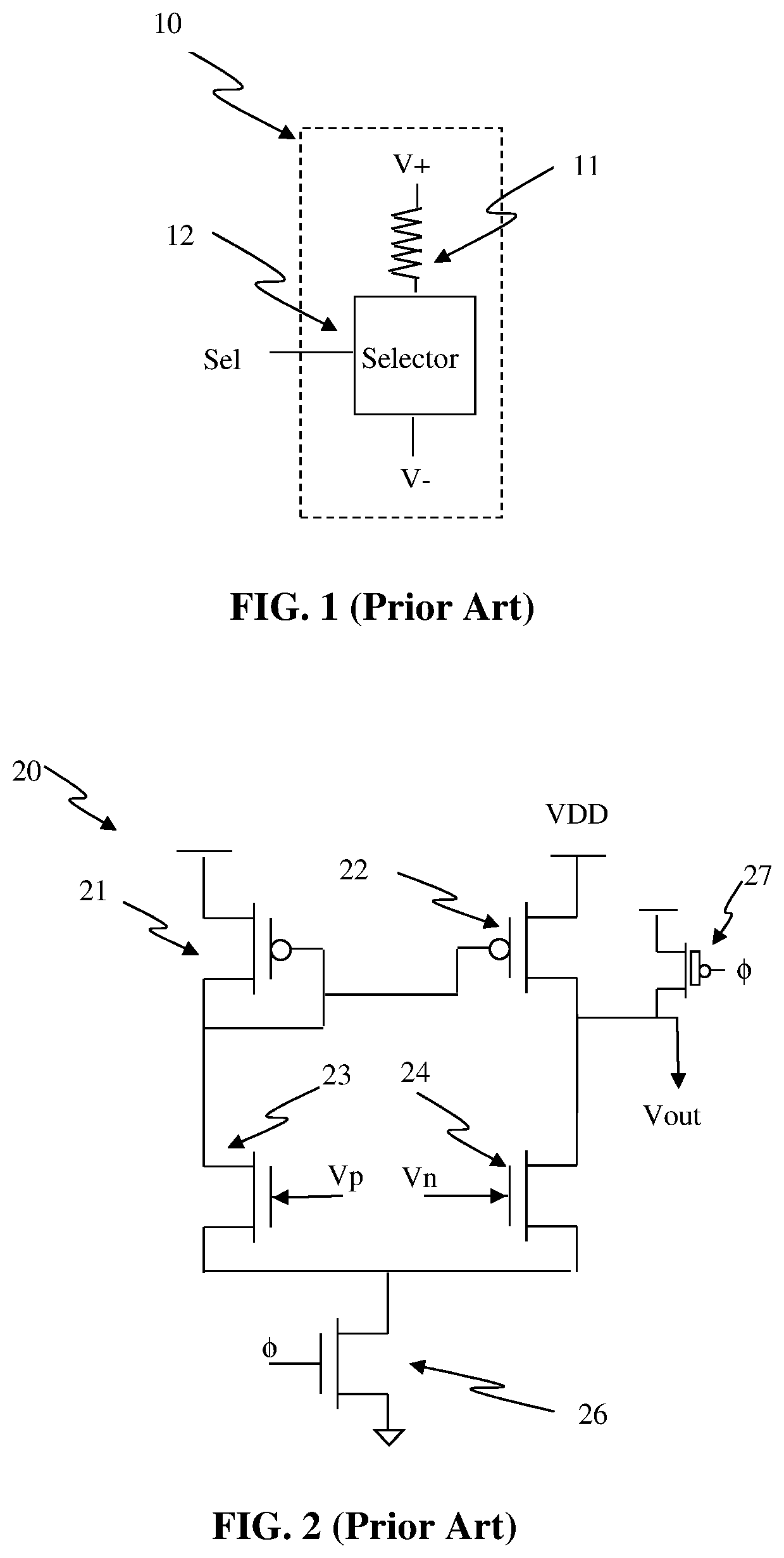
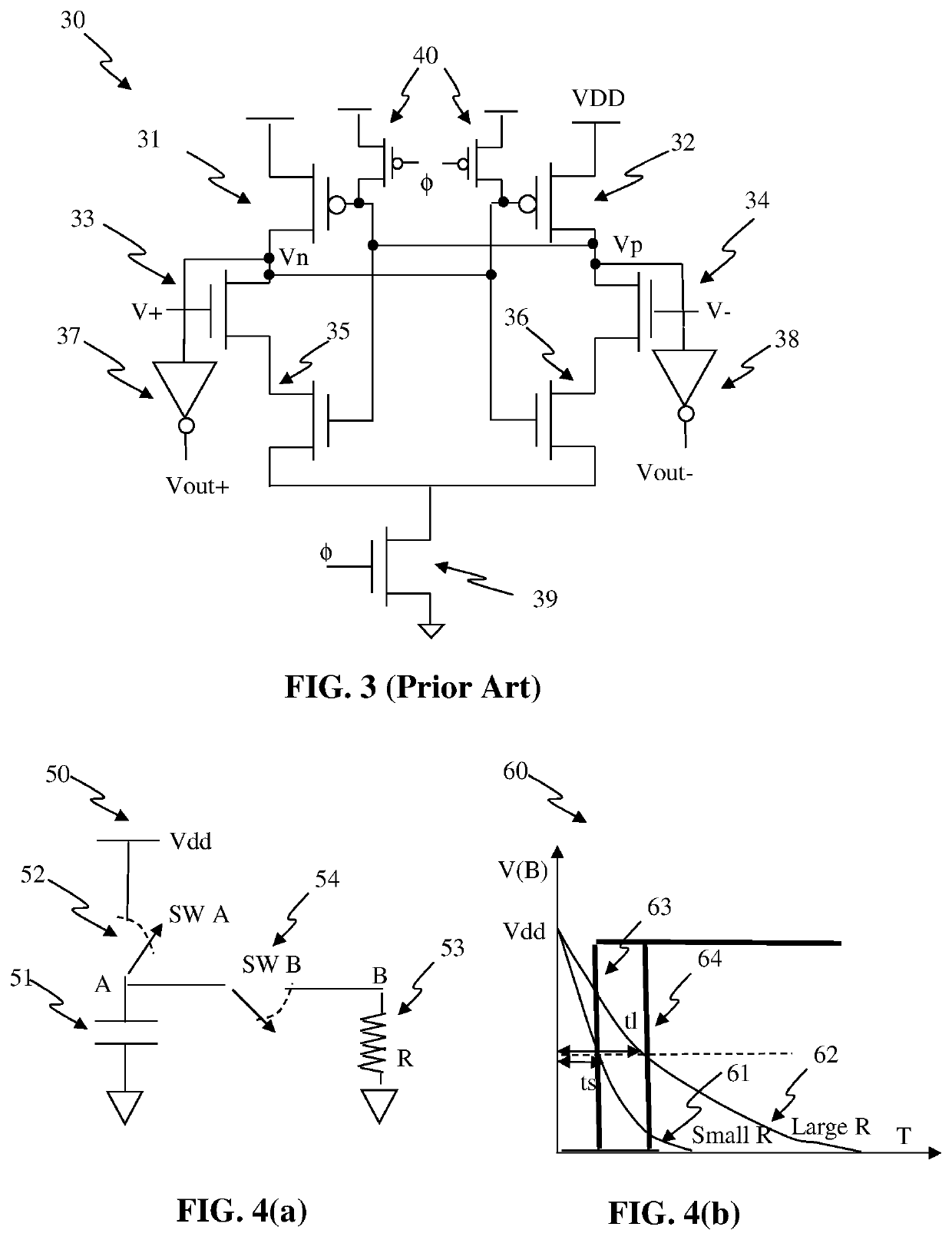
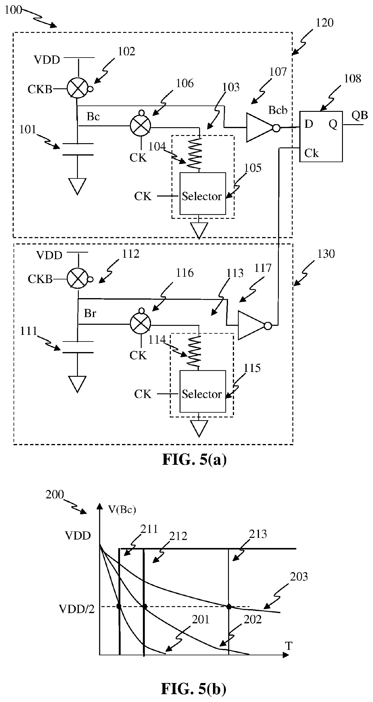
[0045]Embodiments disclosed herein use capacitors discharging through programmable resistance element (PRE) to evaluate a programming state. By comparing a discharging time to reach a predetermined voltage, a resistance of the PRE can be converted into a logic state. The discharging time can be compared with a discharge time provided by a separate unit that used a reference resistance. In one embodiment, an OTP with ultra-low power read can be programmed with a minimum and a maximum program voltage. When programming within the range, the post-program OTP to pre-program resistance ratio can be larger than N, where N>50, so that more sensing techniques can be used to reduce read current. The minimum and the maximum program voltages to achieve the desirable high ratio can be found by programming a portion of OTP cells starting with a relative low program voltage, and incrementing the program voltage until the programmed OTP cells are verified as passed and achieving the high resistance...


PUM


Abstract

An OTP with ultra-low power read can be programmed with a minimum and a maximum program voltage. When programming within the range, the post-program OTP to pre-program resistance ratio can be larger than N, where N>50, so that more sensing techniques, such as single-end sensing, can be used to reduce read current. At least one of the OTP cells can be coupled to a common bitline, which can be further coupled to a first supply voltage lines via a plurality of datalines. The resistance in the at least one OTP cell can be evaluated by strobing at least one comparator output of the discharging bitline/dataline.

Description

CROSS-REFERENCE TO RELATED APPLICATIONS[0001]This application is a Continuation-In-Part of U.S. patent application Ser. No. 16 / 931,314, filed on Jul. 16, 2020 and entitled “ONE-TIME PROGRAMMABLE MEMORIES WITH LOW POWER READ OPERATION AND NOVEL SENSING SCHEME,” which is hereby incorporated herein by reference, which in turn is a Continuation-In-Part of U.S. patent application Ser. No. 16 / 559,560, filed on Sep. 3, 2019 and entitled “PROGRAMMABLE RESISTIVE MEMORIES WITH LOW POWER READ OPERATION AND NOVEL SENSING SCHEME,” which is hereby incorporated herein by reference, which in turn is a Continuation-In-Part of U.S. patent application Ser. No. 15 / 953,422, filed on Apr. 14, 2018 and entitled “LOW POWER READ OPERATION FOR PROGRAMMABLE RESISTIVE MEMORIES,” which is hereby incorporated herein by reference, which claims priority benefit of U.S. Provisional Patent Application No. 62 / 485,895, filed on Apr. 14, 2017 and entitled “CIRCUIT AND SYSTEM OF ULTRA LOW VOLTAGE AND LOW CURRENT READ FO...

Claims


Application Information

Patent Timeline
Patent Type & Authority Applications(United States)
IPC IPC(8): G11C17/18G11C17/16
CPCG11C17/18G11C17/16G11C13/004G11C17/165
Inventor CHUNG, SHINE C.
Owner ATTOPSEMI TECH CO LTD
Why Eureka
Try Eureka