Power conversion module
- Summary
- Abstract
- Description
- Claims
- Application Information
AI Technical Summary
Benefits of technology
Problems solved by technology
Method used
Image

Examples
first embodiment
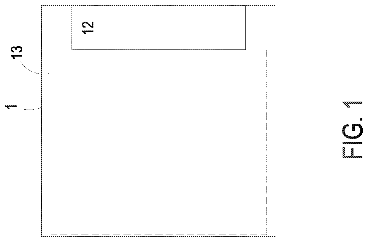
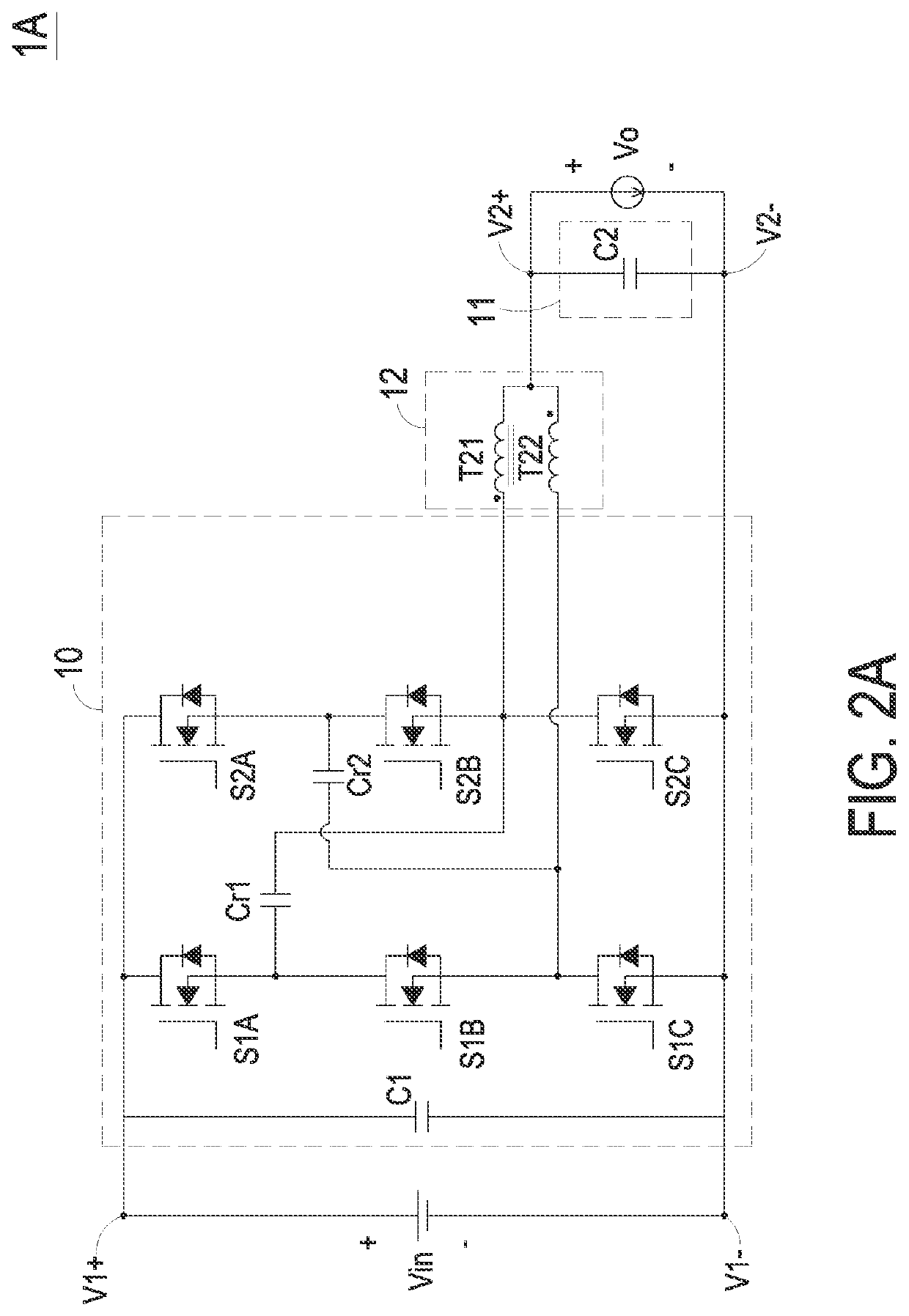
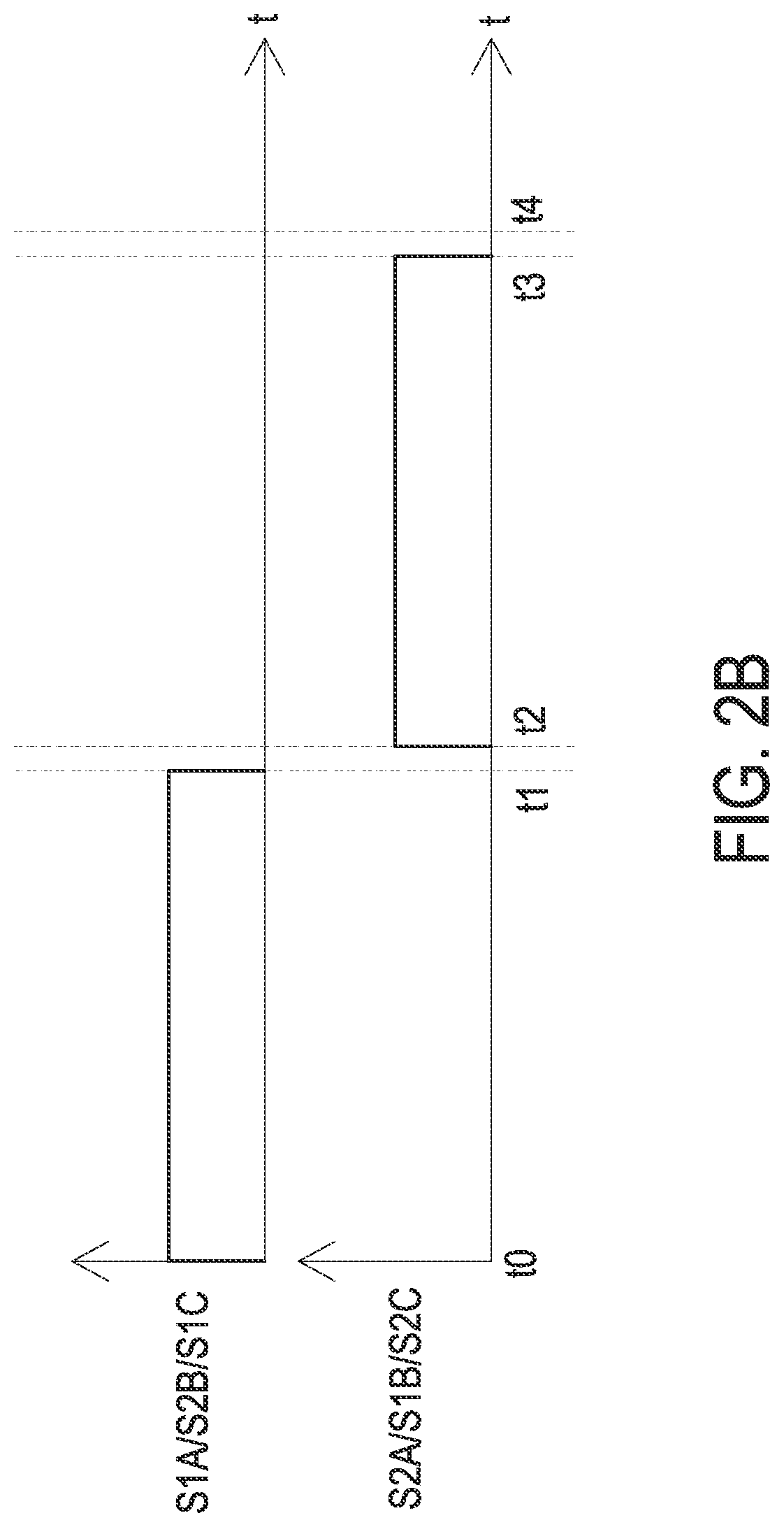
[0024]FIG. 1 schematically illustrates a layout structure of a power conversion module according to the present disclosure. FIG. 2A is a schematic circuit diagram illustrating a first exemplary power conversion circuit of an embodiment of the present disclosure. FIG. 2B is a schematic timing waveform diagram illustrating the time sequence of operating associated switches of the power conversion circuit as shown in FIG. 2A. FIG. 2C is a schematic circuit diagram illustrating the AC loops of the power conversion circuit as shown in FIG. 2B in the time interval between the time point t0 and the time point t1. The power conversion circuit as shown in FIG. 2A can be applied to the power conversion module as shown in FIG. 1.
[0025]In the embodiment, the power conversion module 1 is a non-isolated power conversion module. The non-isolated power conversion module has a resonant and duty-cycle-expandable circuit topology. In the embodiment as shown in FIG. 2A, the power conversion circuit of ...
second embodiment
[0036]FIG. 3 schematically illustrates a layout structure of a power conversion module according to the present disclosure. The circuit diagram as shown in FIG. 2B and the time sequence of operating associated switches as shown in FIG. 2C can be applied to the layout structure of this embodiment. In the time interval between the time point t0 and the time point t1, the power conversion module 1 has three AC loops. The AC current flowing through the third AC loop is equal to the sum of the AC current flowing through the first AC loop and the AC current flowing through the second AC loop. In this embodiment, the third AC loop has the smallest path length, and thus the circumscribed area of the third AC loop is reduced. Consequent1y, the AC loss is effectively reduced. As mentioned above, the third AC loop C is defined by the sixth switch S1C, the first winding T22 and the low-voltage side capacitor C2 collaboratively. In this embodiment, at least one of the sixth switch S1C, the third...
third embodiment
[0037]Please refer to FIGS. 4A and 4B. FIGS. 4A and 4B schematically illustrates a layout structure of a power conversion module according to the present disclosure, in which the two windings are shown. In this embodiment, the two first windings T21 and T21 are planar windings that are mounted on a printed circuit board (not shown). As shown in FIG. 4A, the second terminal of the first winding T21 is electrically connected with the first terminal of the low-voltage side capacitor C2, and the first terminal of the first winding T21 is electrically connected with the first terminal of the third switch S2C. Moreover, a projection area of the third switch S2C with respect to the first winding T21 is partially overlapped with the first winding T21. As shown in FIG. 4B, the second terminal of the first winding T22 is electrically connected with the first terminal of the low-voltage side capacitor C2, and the first terminal of the first winding T22 is electrically connected with the first ...
PUM
 Abstract
Description
Claims
Application Information
PatSnap Eureka turns technology decisions into work you can execute. Powered by our Innovation Knowledge Graph, it runs expert workflows across engineering, life sciences, materials and intellectual property. Get your review-ready output in minutes.


