Optical modulator and optical module using same

Pending Publication Date: 2022-02-10
SUMITOMO OSAKA CEMENT CO LTD
View PDF3 Cites 0 Cited by
  • Summary
  • Abstract
  • Description
  • Claims
  • Application Information

AI Technical Summary

Benefits of technology

[0037]According to the present invention, in an optical modulator, even in a case where a heat source such as an electronic component is disposed close to the optical modulator, it is possible to suppress cha

Problems solved by technology

This configuration is not a technique intended to enlighten a measure for preventing the variation of optical characteristics attributed to heat that is continuously applied from the outside during operation of optical modulators or the degradation of long-term reliability attributed to heat that is continuously applied during the long-term operation of optical modulators.
Therefore, in the optical module, usually, heat is not uniformly applied to the modulator housing 1504.
Such an asymmetric temperature distribution in the modulator housing 1504 is significantly different from a temperature change that is expected by the design concept of the conventional modulator housing 1504, which is “making the wall thicknesses on the four sides the same to suppress deformation”, that is, “a uniform temperature change” in the modulator housing 1504 and may cause characteristic variations and the degradation of long-term reliability that are beyond designers' prediction.
Therefore, particula

Method used


Image

  • Optical modulator and optical module using same
  • Optical modulator and optical module using same
  • Optical modulator and optical module using same

Examples


Example

First Embodiment

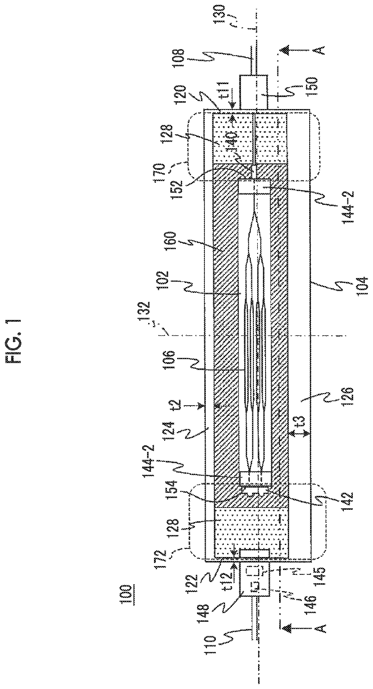
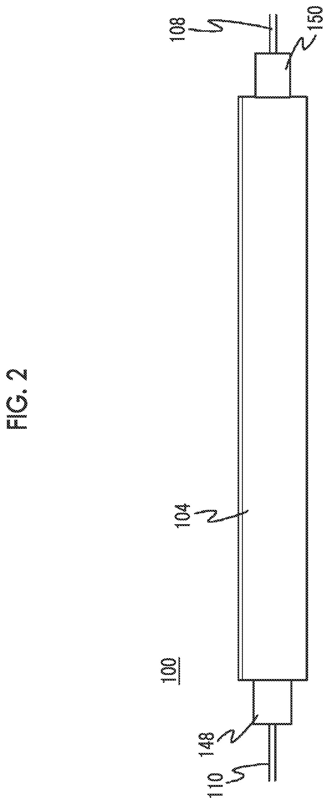
[0057]FIG. 1 is a plan view showing the configuration of an optical modulator 100 according to a first embodiment of the present invention, FIG. 2 is a side view of the optical modulator 100, and FIG. 3 is a cross-sectional view of the optical modulator 100 shown in FIG. 1 taken along the line AA.

[0058]The optical modulator 100 includes an optical modulation element 102, a modulator housing 104 that accommodates the optical modulation element 102, an input optical fiber 108 that inputs light to the optical modulation element 102, and an output optical fiber 110 that guides light output from the optical modulation element 102 to the outside of the modulator housing 104.

[0059]It should be noted that, since the modulator housing 104 is airtightly sealed, it is not possible to actually observe the inside of the modulator housing 104; however, in FIG. 1, configuration elements in the modulator housing 104 are indicated with solid lines in order to facilitate the understan...

Example

Second Embodiment

[0090]Next, a second embodiment of the present invention will be described. FIG. 4 is a plan view showing the configuration of an optical modulator 400 according to the second embodiment. In addition, FIG. 5 is a cross-sectional view of the optical modulator 400 shown in FIG. 4 taken along the line BB. In FIG. 4 and FIG. 5, for the same configuration element and wall thickness as in the optical modulator 100 according to the first embodiment in FIG. 1 and FIG. 3, the same reference sign as in FIG. 1 and FIG. 3 is used, and the description of the above-described optical modulator 100 will be incorporated. In addition, the side surface appearance of the optical modulator 400 is regarded as the same as the side surface appearance of the optical modulator 100 shown in FIG. 2. In addition, in FIG. 4, in order to facilitate the understanding of the configuration of the optical modulator 400, similar to FIG. 1, the internal structure, which cannot be observed in a state wh...

Example

Third Embodiment

[0096]Next, a third embodiment of the present invention will be described. FIG. 6 is a plan view showing the configuration of an optical modulator 600 according to the third embodiment. In addition, FIG. 7 is a cross-sectional view of the optical modulator 600 shown in FIG. 6 taken along the line CC. In FIG. 6 and FIG. 7, for the same configuration element and wall thickness as in the optical modulators 100 and 400 according to the first and second embodiments in FIG. 1, FIG. 2, FIG. 3, FIG. 4, and FIG. 5, the same reference sign as in FIG. 1, FIG. 2, FIG. 3, FIG. 4, and FIG. 5 is used, and the description of the above-described optical modulators 100 and 400 will be incorporated. In addition, the side surface appearance of the optical modulator 600 is regarded as the same as the side surface appearance of the optical modulator 100 shown in FIG. 2. In addition, in FIG. 6, in order to facilitate the understanding of the configuration of the optical modulator 600, simi...


PUM


Abstract

An optical modulator includes an optical modulation element including an optical waveguide formed on a substrate and a housing that accommodates the optical modulation element, the housing has a bottom surface wall having a quadrilateral shape in a plan view, first and second long side walls that are connected to two opposite edges of the bottom surface wall, and first and second short side walls that are shorter than the first and second long side walls and are connected to two other opposite edges of the bottom surface wall. An average wall thickness of the second long side wall is equal to or larger than an average wall thickness of the first long side wall. At least one of the first and second short side walls has an average thickness that is thinner than the average thickness of the first long side wall.

Description

TECHNICAL FIELD[0001]The present invention relates to an optical modulator and an optical module that performs an optical communication operation using the optical modulator.BACKGROUND ART[0002]In recent years, the digital coherent transmission technology, which started to be applied to long-distance optical communication, also has been continuously applied to metro optical communication such as medium-distance and short-distance optical communication due to an additionally increasing communication demand. In such digital coherent transmission, dual polarization-quadrature phase shift keying (DP-QPSK) modulators in which a LiNbO3 (hereinafter, referred to as LN) substrate is typically used are used as optical modulators. Hereinafter, optical modulators in which a LiNbO3 substrate is used will be referred to as LN modulators.[0003]Such an optical modulator is used in a state of being mounted in an optical module that performs an optical communication operation together with, for exam...

Claims


Application Information

Patent Timeline
IPC IPC(8): G02F1/225
CPCG02F1/225G02F1/212G02F2202/20
Inventor MIYAZAKI, NORIKAZUSUGAMATA, TORU
Owner SUMITOMO OSAKA CEMENT CO LTD
Why Eureka
Try Eureka